Power device integration on a common substrate

a technology of power devices and substrates, applied in the field of electrical circuits, can solve problems such as high product cos

Active Publication Date: 2014-09-30
SILANNA ASIA
View PDF27 Cites 24 Cited by
  • Summary
  • Abstract
  • Description
  • Claims
  • Application Information

AI Technical Summary

Benefits of technology

[0006]Embodiments of the invention provide novel semiconductor structure and techniques for facilitating the integration of circuits and / or components (e.g., drivers and power switches) on the same silicon substrate as corresponding control circuitry for implementing a power control device. To accomplish this, embodiments of the invention exploit features of a BiCMOS IC fabrication technology implemented on silicon-on-insulator (SOI) substrates with dielectric lateral isolation.

Problems solved by technology

Consequently, an allocation of a large die area to the power switch leads to a high product cost, which is undesirable.

Method used


Image

  • Power device integration on a common substrate
  • Power device integration on a common substrate
  • Power device integration on a common substrate

Examples


Embodiment Construction

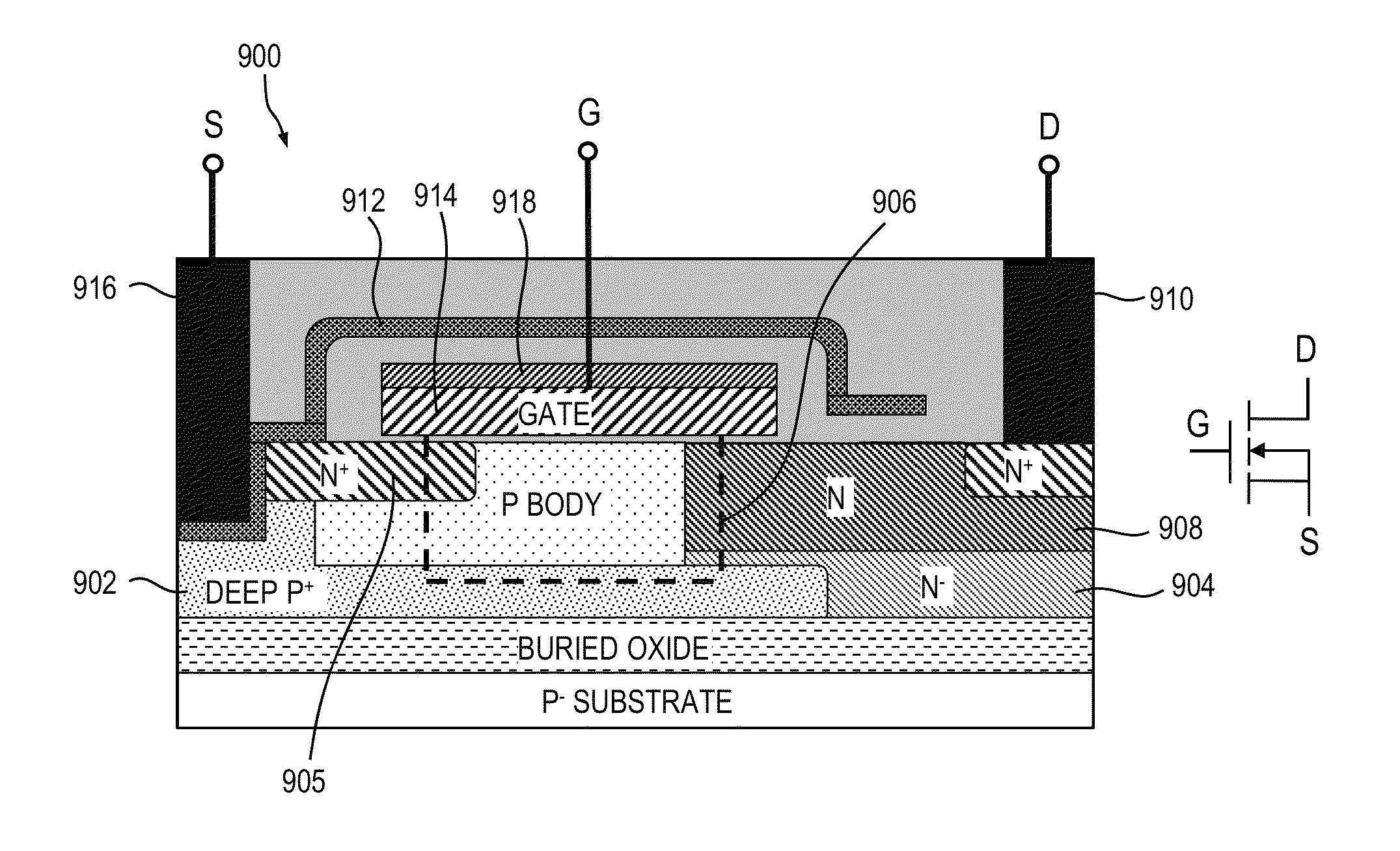
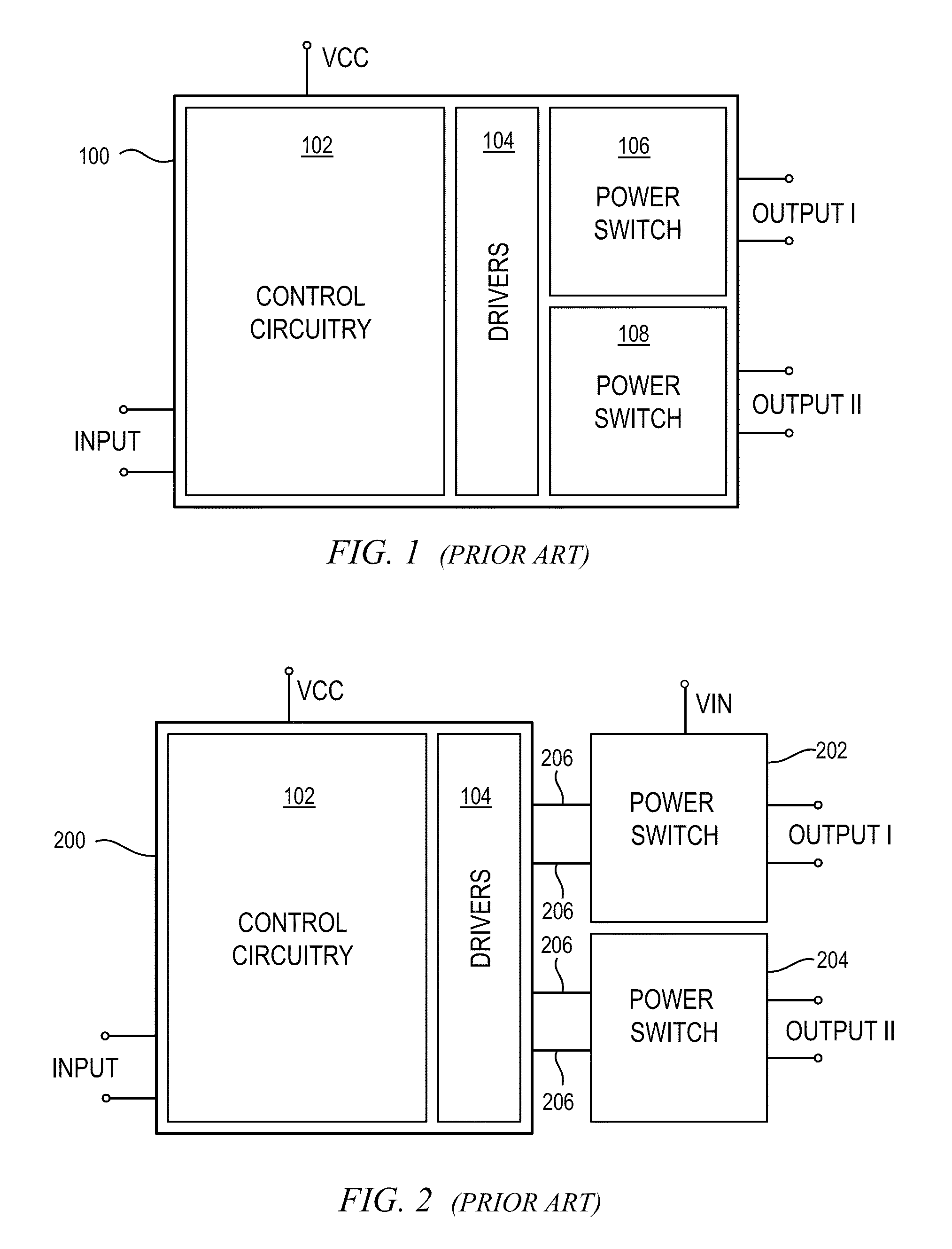
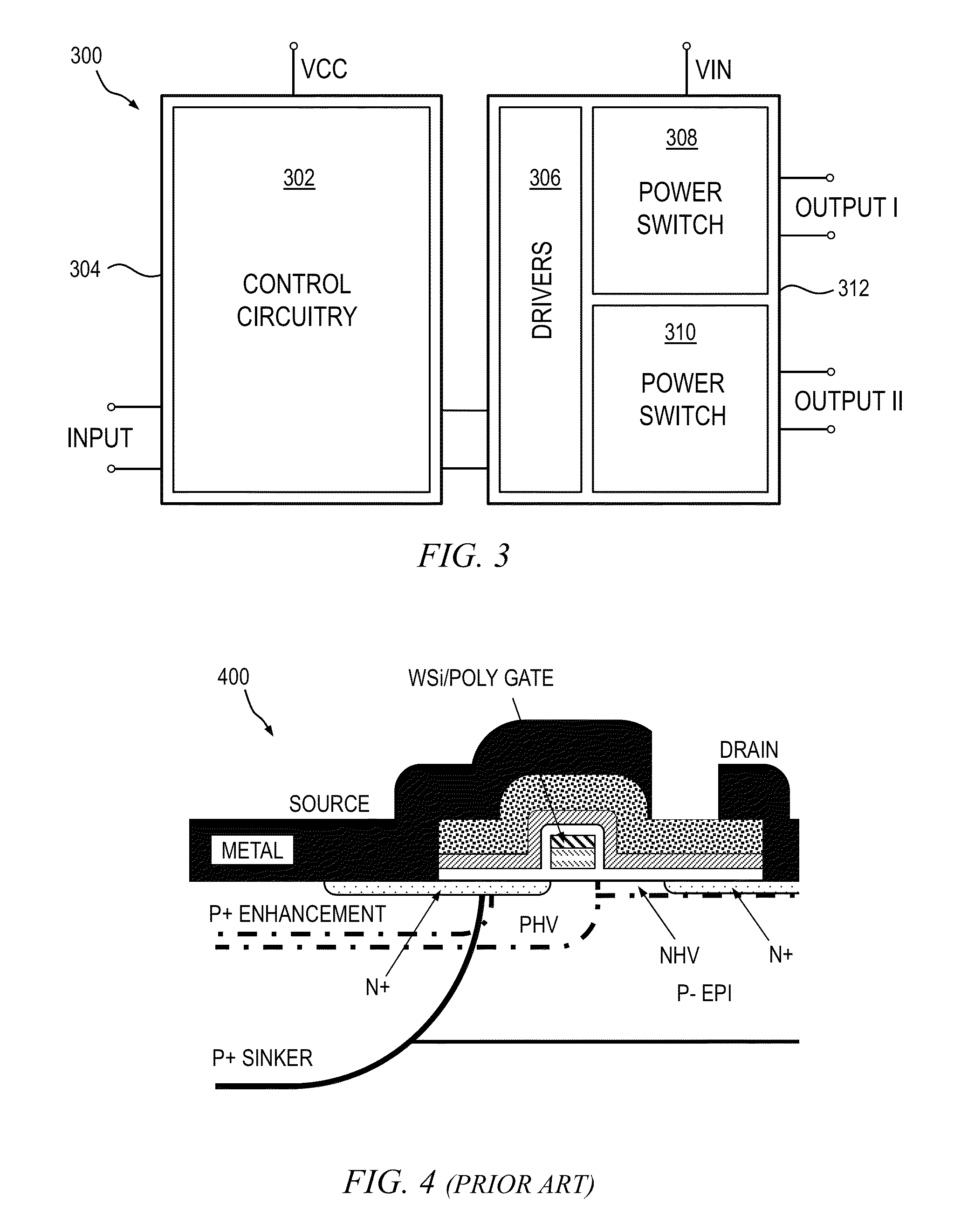
[0042]Embodiments of the invention will be described herein in the context of illustrative power management circuits and semiconductor fabrication methods for forming one or more components suitable for use in the illustrative power management circuits. It should be understood, however, that embodiments of the invention are not limited to the particular circuits and / or methods shown and described herein. Rather, embodiments of the invention are more broadly related to techniques for fabricating an integrated circuit in a manner which achieves high-frequency performance for a variety applications, such as, for example, radio frequency (RF) signal amplification, and advantageously reduces the physical size and cost of external components which may be used in conjunction with embodiments of the invention, such as, for example, a DC-DC power supply, an output filter, among other benefits. Moreover, it will become apparent to those skilled in the art given the teachings herein that numer...


PUM


Abstract

A MOSFET includes an active region formed on an SOI substrate. A buried well is formed in the active region. A drain region having the first conductivity type is formed in the active region and spaced laterally from a source region and the buried well. A body region is formed in the active region between the source and drain regions on the buried well, and a drift region is formed in the active region between the drain and body regions on at least a portion of the buried well. A shielding structure is formed proximate the upper surface of the active region, overlapping a gate. During conduction, the buried well forms a PN junction with the drift region which, in conjunction with the shielding structure, depletes the drift region. The MOSFET is configured to sustain a linear mode of operation of an inversion channel formed under the gate.

Description

CROSS-REFERENCE TO RELATED APPLICATION(S)[0001]This patent application is a continuation-in-part of U.S. application Ser. No. 13 / 887,704 filed on May 6, 2013, entitled “Power Device Integration on a Common Substrate,” which claims the benefit of U.S. Provisional Patent Application Ser. No. 61 / 677,660 filed on Jul. 31, 2012, the disclosures of which are incorporated herein by reference in their entireties for all purposes.FIELD OF THE INVENTION[0002]The present invention relates generally to electronic circuits, and more particularly relates to power device integration.BACKGROUND OF THE INVENTION[0003]Modern portable electronic devices, including, but not limited to, smart phones, laptop and tablet computing devices, netbooks, etc., are battery operated and generally require power supply components for stabilizing the supply voltage applied to subsystems in the devices, such as, for example, microprocessors, graphic displays, memory chips, etc. The required power range is often betwe...

Claims


Application Information

Patent Timeline
Patent Type & Authority Patents(United States)
IPC IPC(8): H01L29/76
CPCH01L29/945H01L29/7302H01L29/402H01L29/8605H01L29/41766H01L29/1095H01L29/1083H01L29/66659H01L29/7835H01L29/4933H01L29/66371H01L29/0626H01L29/4236H01L29/7824H01L29/8611H01L29/1087H01L2924/13091H01L29/0847H01L29/8725H01L29/42304H01L29/872H01L27/1203H01L29/735H01L29/66681H01L29/782H01L29/41758H01L29/66696H01L29/66704H01L29/7838H01L29/7839H01L29/0878H01L2924/00
Inventor KOREC, JACEK
Owner SILANNA ASIA
Why Eureka
Try Eureka