Surface plasmon enhanced optical devices for integrated photonics

a surface plasmon and photonics technology, applied in the field of optical devices, can solve the problems of increased device density, large loss, destructive interference and therefore isolation, etc., and achieve the effect of reducing the size and cost of the optical system, and increasing the complexity of the optical system

Inactive Publication Date: 2014-09-30
PHYSICAL SCI
View PDF6 Cites 17 Cited by
  • Summary
  • Abstract
  • Description
  • Claims
  • Application Information

AI Technical Summary

Benefits of technology

[0020]As the complexity of optical system increases, multiple optical functions, including but not limited to optical isolation, frequency conversion, and amplitude modulation, can be monolithically integrated onto a single material substrate to reduce the size and cost of the optical system. Lattice mismatch between semiconductors (such as InP and GaAs used in photonic chips) and magneto-optic materials (such as BIG and YIG) used in optical isolators and nonlinear materials (such as lithium niobate) used in frequency converters and amplitude modulators can be overcome.
[0021]Surface plasmon integrated circuits and devices offer several attractive features such as strong confinement of optical fields, the ability to simultaneously transport photonic and electronic signals, tolerance for sharp bending, and compatibility with existing semiconductor materials and manufacturing processes. Magneto-optic surface plasmon devices can exploit the ability to use the surface plasmon guiding metal as a current-carrying wire to generate magnetic fields that interact with the surface plasmon propagation characteristics. This current-induced localized magnetic field is well suited for optical devices such as high-bandwidth amplitude modulators and other optical devices such as optical isolators, frequency modulators, couplers, splitters, combiners and the like.

Problems solved by technology

Optical isolators can be used in optical systems since backscattered light creates noise and instability in laser sources, particularly in integrated platforms where the potential for backscattering increases with device density.
In the reverse direction, a nonreciprocal phase shift in one or both arms produces destructive interference and therefore isolation.
In the reverse direction, the nonreciprocity results in a larger loss resulting in isolation.
The birefringence method is limited to materials and wavelengths with specific properties, and not generally applicable to integrated photonic devices.
Fabrication methods for QPM devices, however, require periodic patterning of crystal structures and have only been demonstrated for a small class of ferroelectric materials and semiconductors such as GaAs and ZnSe.
When the optical fields in the interferometer arms are recombined, destructive interference occurs as a result of the induced phase shift.
The bandwidth in thermo-optic based devices can be low as a result of the slow heating process.

Method used


Image

  • Surface plasmon enhanced optical devices for integrated photonics
  • Surface plasmon enhanced optical devices for integrated photonics
  • Surface plasmon enhanced optical devices for integrated photonics

Examples


Embodiment Construction

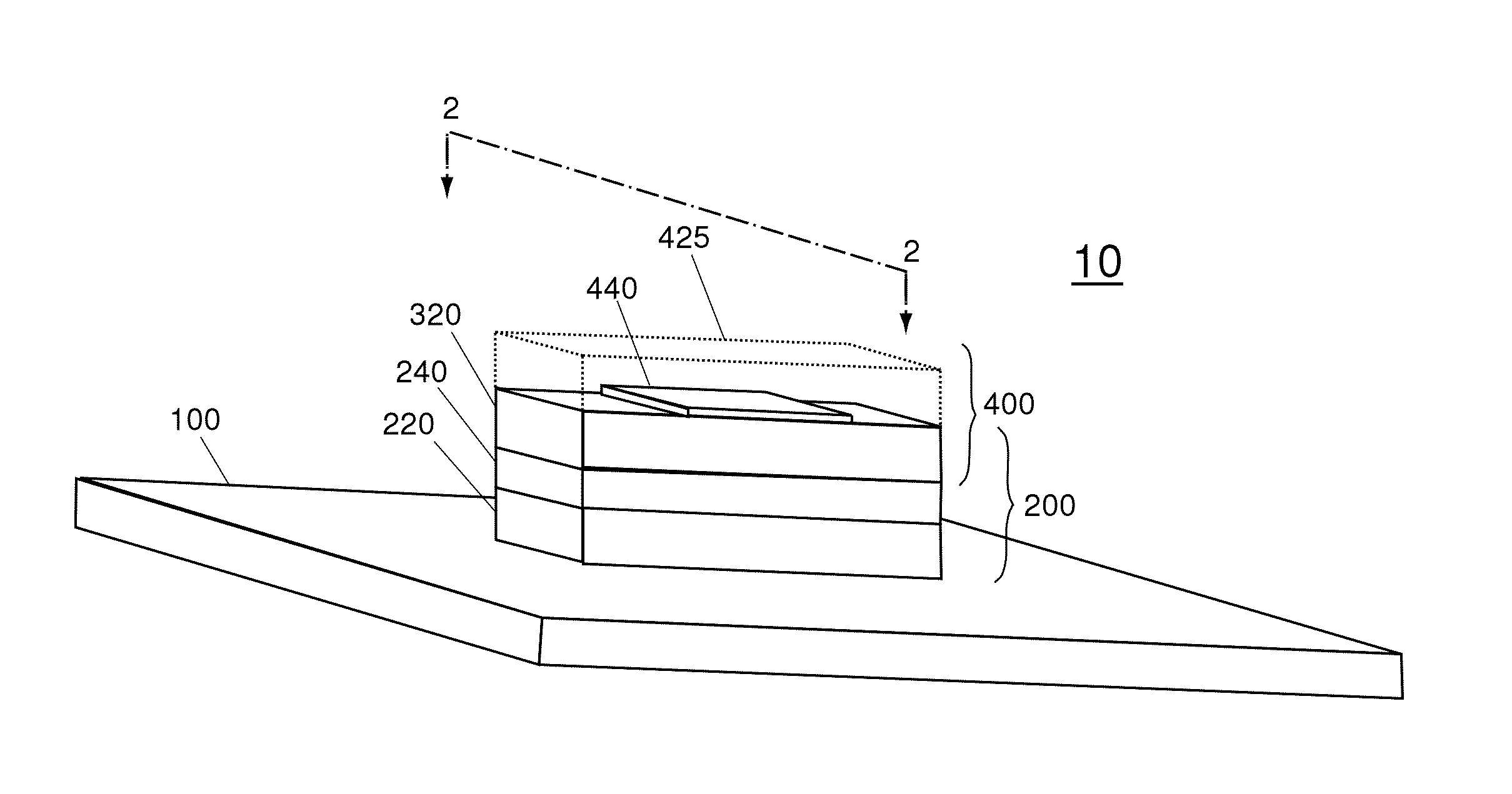
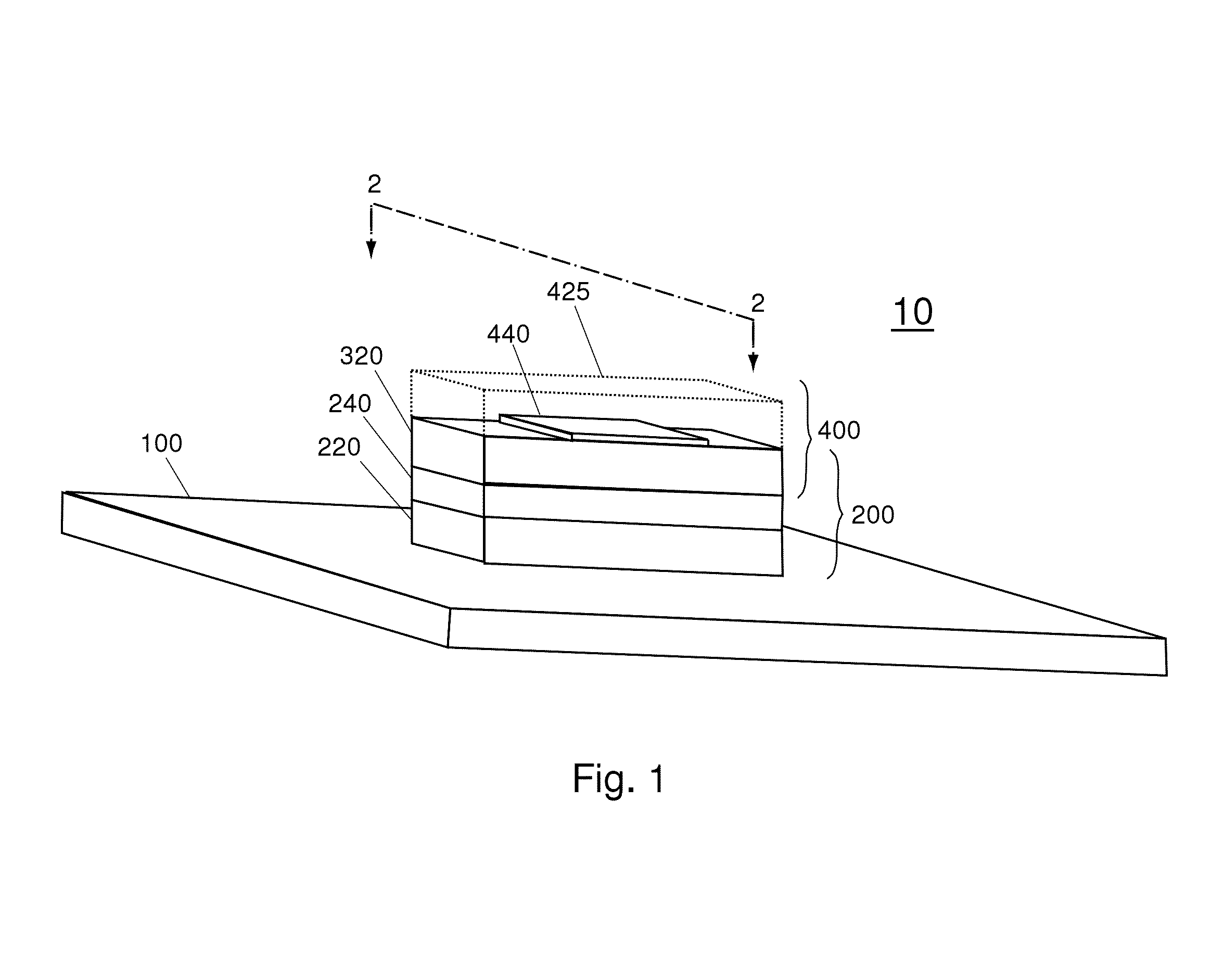
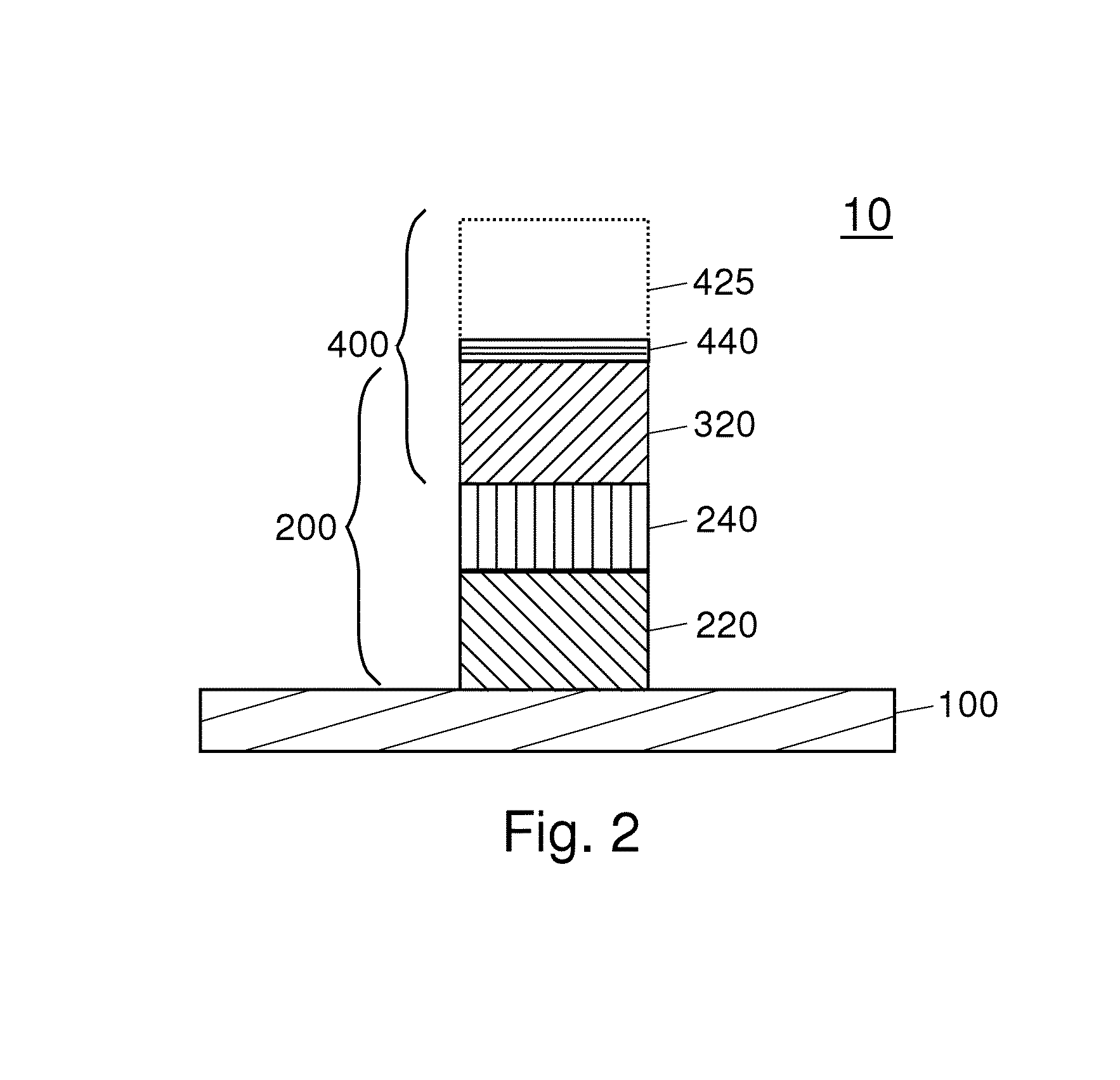
[0069]FIG. 1 shows an optical device 10, e.g., an isolator, fabricated on substrate 100 and exploits a nonreciprocal coupling from a dielectric waveguide 200 into a surface plasmon waveguide 400 to achieve large isolation in the reverse direction and low insertion loss in the forward direction. FIG. 2 depicts the optical device 10 in cross sectional view with the ridge width. The two waveguides are designed to share a common cladding 320. The dielectric waveguide 200 includes three dielectric layers referred to as dielectric waveguide cladding 220, dielectric waveguide core 240, and the common cladding 320. The surface plasmon waveguide 400 includes three layers referred to as effective surface plasmon cladding 425, surface plasmon core 440, and the common cladding 320.

[0070]The optical device 10 is compatible with fabrication techniques developed for the semiconductor industry on substrate 100. In various embodiments, substrate 100 can be InP, GaAs, Si, GaSb, GaN, or other like mat...


PUM

PropertyMeasurementUnit
insertion lossaaaaaaaaaa
thicknessaaaaaaaaaa

Abstract

An optical device for integrated photonic applications includes a substrate, a dielectric waveguide and a surface plasmon waveguide. The dielectric waveguide includes a dielectric waveguide core disposed relative to a dielectric waveguide cladding and a common cladding. The surface plasmon waveguide includes a surface plasmon waveguide core disposed relative to the common cladding and a surface plasmon waveguide cladding. The common cladding couples the dielectric waveguide and the surface plasmon waveguide.

Description

CROSS-REFERENCE TO RELATED APPLICATIONS[0001]This application claims the benefit of and priority to U.S. provisional patent application No. 61 / 152,377 filed Feb. 13, 2009, which is owned by the assignee of the instant application and the disclosure of which is incorporated herein by reference in its entirety.STATEMENT OF GOVERNMENT INTEREST[0002]This invention was made with government support by the Defense Advanced Research Projects Agency and U.S. Army Aviation & Missile Command under Contract No. W31P4Q-08-C-0233 and Contract No. W31P4Q-09-C-0318. The Government has certain rights in the invention.FIELD OF THE INVENTION[0003]This invention relates generally to optical devices suitable for integrated photonic applications, and more particularly to surface plasmon enhanced optical devices.BACKGROUND OF THE INVENTION[0004]Integrated photonics offer the promise of combining many optical devices on a substrate, leading to miniaturization and increased functionality on a chip. Optical ...

Claims


Application Information

Patent Timeline
Patent Type & Authority Patents(United States)
IPC IPC(8): G02F1/295G02B6/12G02B6/02B82Y20/00G02B6/122G02F1/01G02F1/095
CPCG02B6/1226G02F1/0955G02F1/011B82Y20/00G02B2006/12097G02F2203/10
Inventor MONTOYA, JUANALLEN, MARK G.HENSLEY, JOEL M.PARAMESWARAN, KRISHNAN R.RAM, RAJEEV
Owner PHYSICAL SCI
Why Eureka
Try Eureka