Scan compression architecture with bypassable scan chains for low test mode power

a compression architecture and scan chain technology, applied in the direction of electronic circuit testing, measurement devices, instruments, etc., can solve the problems of reducing the efficiency of scanning devices under test, affecting the operation of scanning devices, and consuming much more power than the designed operating power, so as to minimize the overall toggle activity, minimize power consumption, and save considerable power

Active Publication Date: 2014-10-07
TEXAS INSTR INC
View PDF20 Cites 3 Cited by
  • Summary
  • Abstract
  • Description
  • Claims
  • Application Information

AI Technical Summary

Benefits of technology

[0006]These difficulties in test operations can be mitigated by the present invention. This invention permits selective bypassing of each of the serial scan chains (often called a STUMPS channel). The bypassed serial chains can be loaded with constant of low toggle data supplied within the integrated circuit. An example of this invention scans in 0s so that every flip flop goes through a 0 to 0 transition. Alternately scanning in all 1s causes every flip flop to go through a 1 to 1 transition. Where the bypassed serial scan chains have data inversion logic in the scan path, the scanned in sequence can have a set of 0s and 1′ that minimize the overall toggle activity to minimize power consumption. Because a serial scan chain generally includes hundreds of flip-flops, directing constant or low toggle data into the serial scan chain can save considerable power. While bypassing a serial scan chain, the normal scan-in data is directed to a bypass flip-flop to ensure an unbroken scan path between decompressor and compactor.
[0007]In another aspect of the invention, each serial scan chain of the device under test is equipped with such a bypass. The number and identity of serial scan chains bypassed during a particular test can be changed dynamically dependent upon the semiconductor process variations of a particular integrated circuit. This enables an optimal test to be preformed for integrated circuits having design characteristics and differing semiconductor process variations.

Problems solved by technology

There are some disadvantages to this scanned based test technique.
This has adverse implications for the power consumption of the device.
Scanning a device under test may consume much more power than the designed operating power.
This may adversely impact the thermal design of the integrated circuit.
Switching a large number of flip-flops simultaneously may cause improper operation of the scan chain due to large IR voltage drops.

Method used


Image

  • Scan compression architecture with bypassable scan chains for low test mode power
  • Scan compression architecture with bypassable scan chains for low test mode power
  • Scan compression architecture with bypassable scan chains for low test mode power

Examples


Embodiment Construction

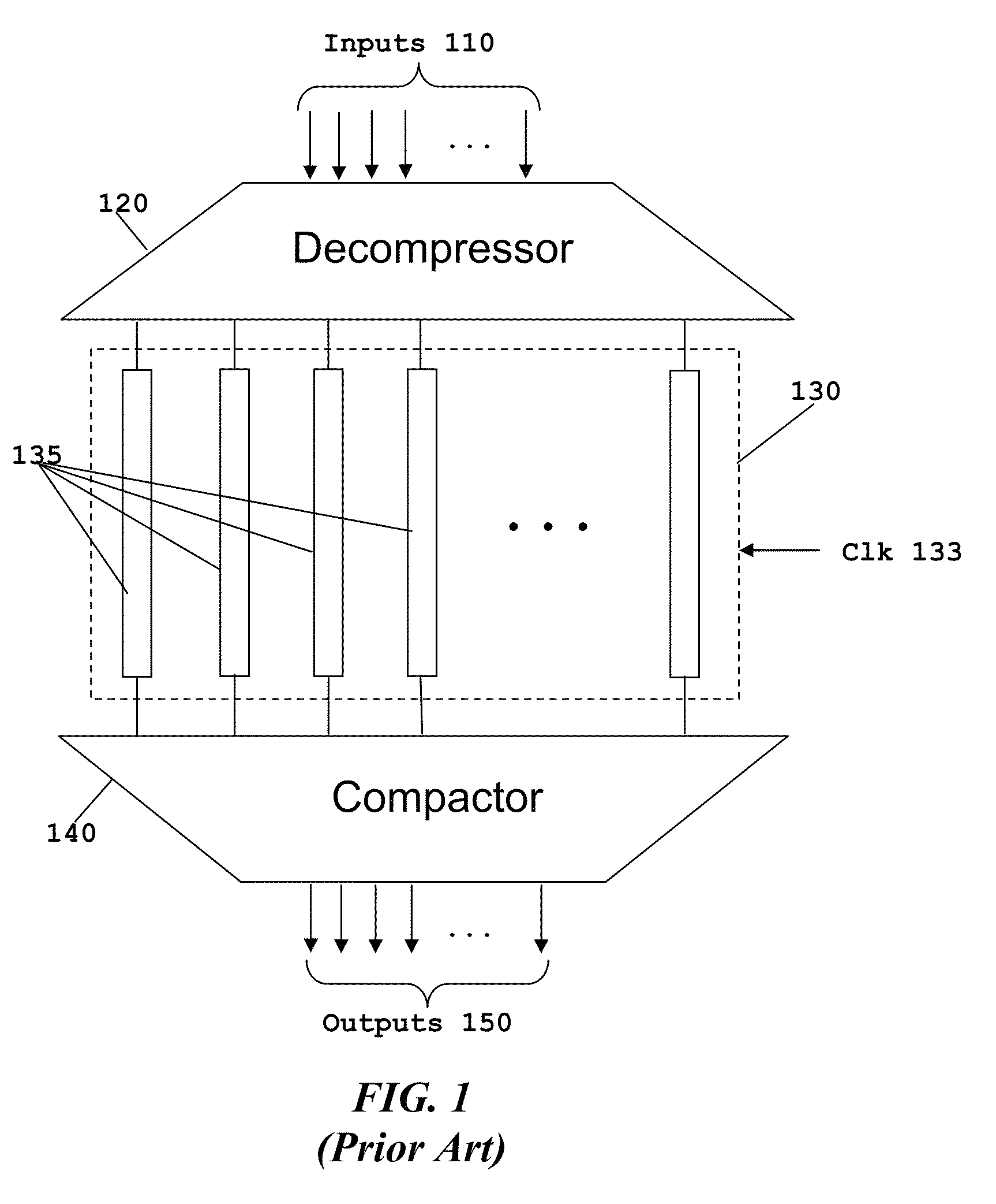
[0019]FIG. 1 illustrates the prior art compressed input data testing technique. An external tester (not illustrated) supplies compressed test data to inputs 110. Decompressor 120 decompresses this compressed test data and divides it into plural data streams. Decompressor 120 supplies these plural data streams to plural serial scan chains 135 of the circuit under test 130. Each serial scan chain 135 produces an output supplied to compactor 140. Compactor 140 compresses these data streams into a smaller set of outputs 150. Outputs 150 are supplied to the external tester for comparison with expected output data. This comparison indicates whether circuit under test 130 is operating as expected.

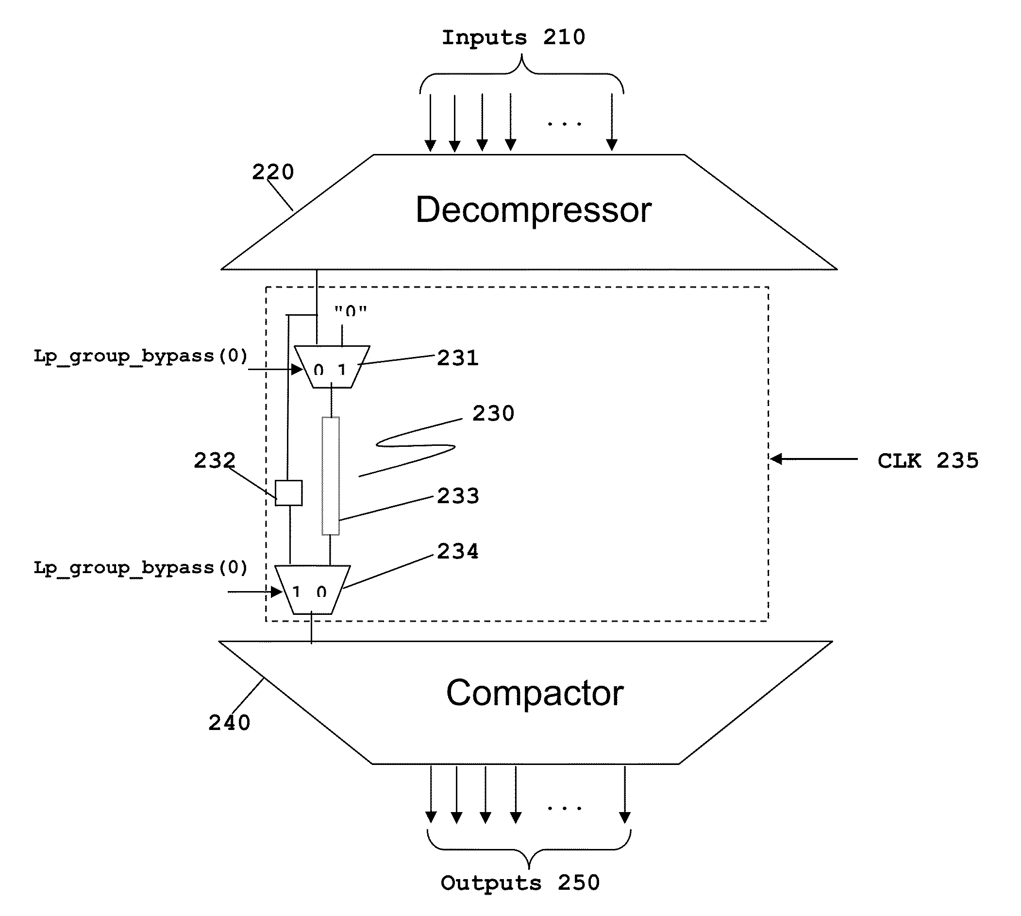
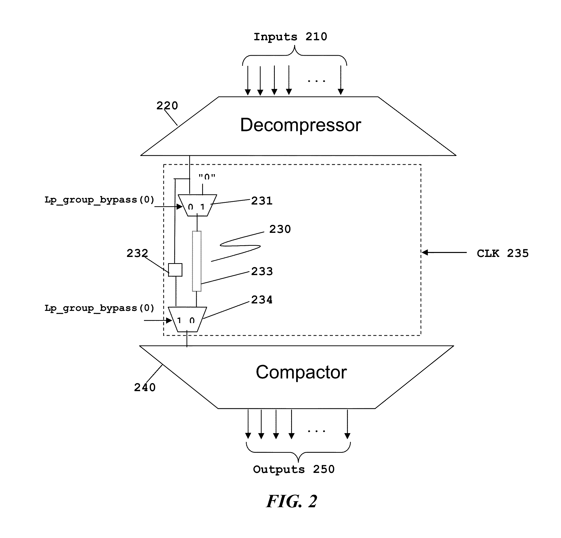
[0020]FIG. 2 illustrates key points of the present invention. FIG. 2 illustrates decompressor 220 similar to FIG. 1 receiving inputs 210. FIG. 2 further illustrates compactor 240 similar to FIG. 1. FIG. 2 illustrates a single serial scan chain 230 as an example. Serial scan chain 230 is representa...


PUM


Abstract

This invention permits selectively bypasses serial scan chains. Constant or low toggle data is directed to the bypassed serial scan chain, thus reducing power consumption. The number and identity of serial scan chains bypassed during a particular test can be changed dynamically dependent upon the semiconductor process variations of a particular integrated circuit. This enables an optimal test to be preformed for integrated circuits having differing semiconductor process variations.

Description

CLAIM OF PRIORITY[0001]This application claims priority under 35 U.S.C. 119(e)(1) to U.S. Provisional Application No. 61 / 236,753 filed Aug. 25, 2009.TECHNICAL FIELD OF THE INVENTION[0002]The technical field of this invention is integrated circuit testing and more specifically testing using scan chains while mitigating power consumed by the integrated circuit during testing.BACKGROUND OF THE INVENTION[0003]Semiconductor manufacturers typically test integrated circuits to weed out defective integrated circuits after fabrication. It is typical in the art to divide the whole device under test into plural sets of scan chains consisting of flip-flops storing various states of the device. These flip-flops generally correspond to state storing portions of the device. Each scan chain has an input, a serial set of flip-flops holding a subset of the states of the device under test and an output. Such serial scan chains permit testing of the circuit under test as follows. Data is loaded into th...

Claims


Application Information

Patent Timeline
Patent Type & Authority Patents(United States)
IPC IPC(8): G01R31/28G01R31/3177G01R31/3185
CPCG01R31/3177G01R31/318547
Inventor RAVI, SRIVATHSTIWARI, RAJESH KUMARPAREKHJI, RUBIN AJIT
Owner TEXAS INSTR INC
Why Eureka
Try Eureka