Method for making three-dimensional nano-structure array

a three-dimensional nano-structure and array technology, applied in the field of three-dimensional nano-structure arrays, can solve the problems of complex three-dimensional nano-structure fabrication process, high cost of lithography, and difficult fabrication of three-dimensional nano-structures,

Active Publication Date: 2014-10-21
TSINGHUA UNIV +1
View PDF13 Cites 2 Cited by
  • Summary
  • Abstract
  • Description
  • Claims
  • Application Information

AI Technical Summary

Benefits of technology

[0005]Nano materials can be one-dimensional such as carbon nanotube, or two-dimensional such as grapheme. A three-dimensional nano-structure, such as a three-dimensional nano-structure array, is difficult to fabricate. A method for making the three-dimensional nano-structure array usually includes lithographing. However, the cost of lithography is expensive, and the three-dimensional nano-structure fabrication process is complicated.

Problems solved by technology

A three-dimensional nano-structure, such as a three-dimensional nano-structure array, is difficult to fabricate.
However, the cost of lithography is expensive, and the three-dimensional nano-structure fabrication process is complicated.

Method used


Image

  • Method for making three-dimensional nano-structure array
  • Method for making three-dimensional nano-structure array
  • Method for making three-dimensional nano-structure array

Examples


Embodiment Construction

[0018]The disclosure is illustrated by way of example and not by way of limitation in the figures of the accompanying drawings in which like references indicate similar elements. It should be noted that references to “an” or “one” embodiment in this disclosure are not necessarily to the same embodiment, and such references mean at least one.

[0019]References will now be made to the drawings to describe, in detail, various embodiments of the present three-dimensional nano-structure arrays and methods for making the same.

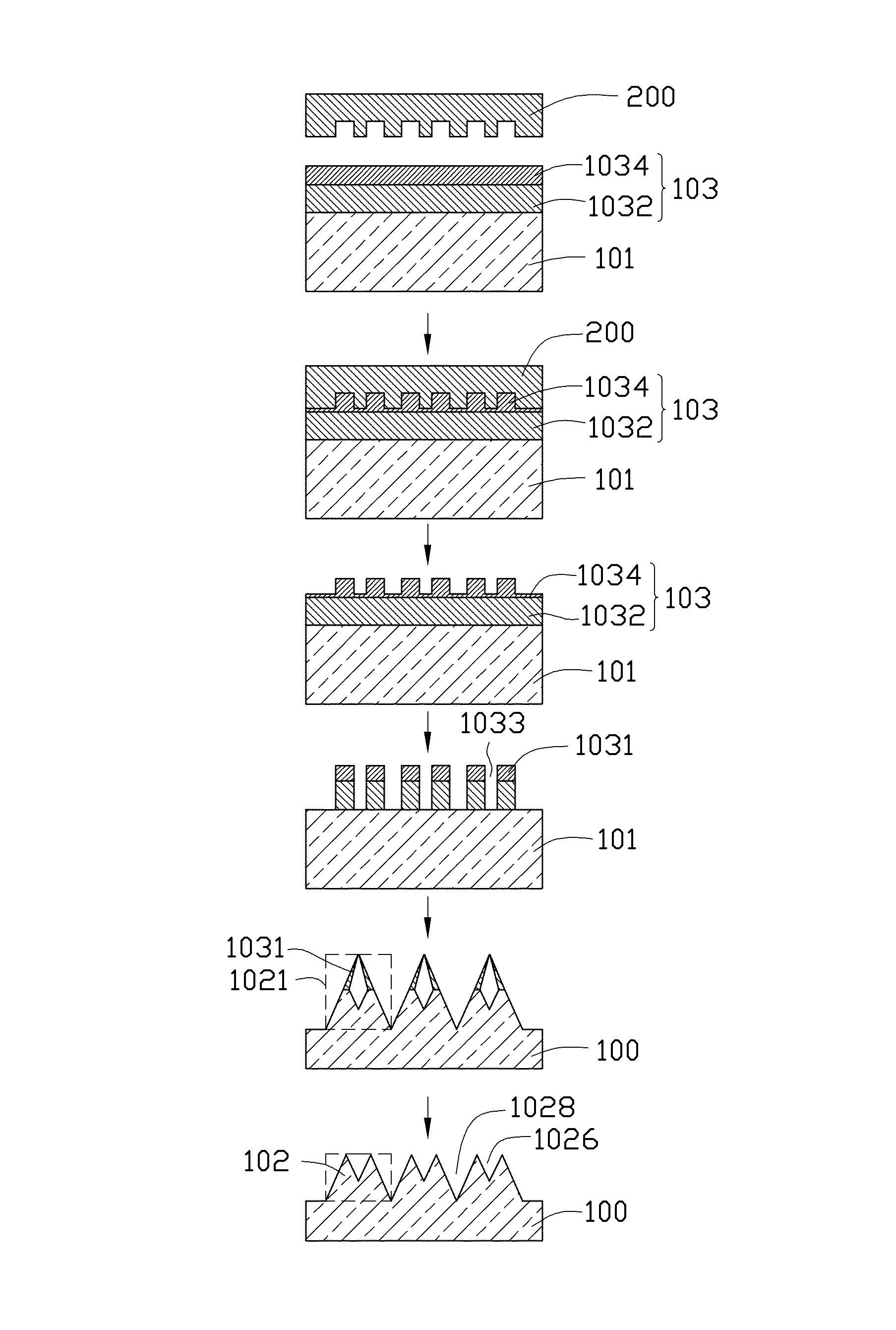
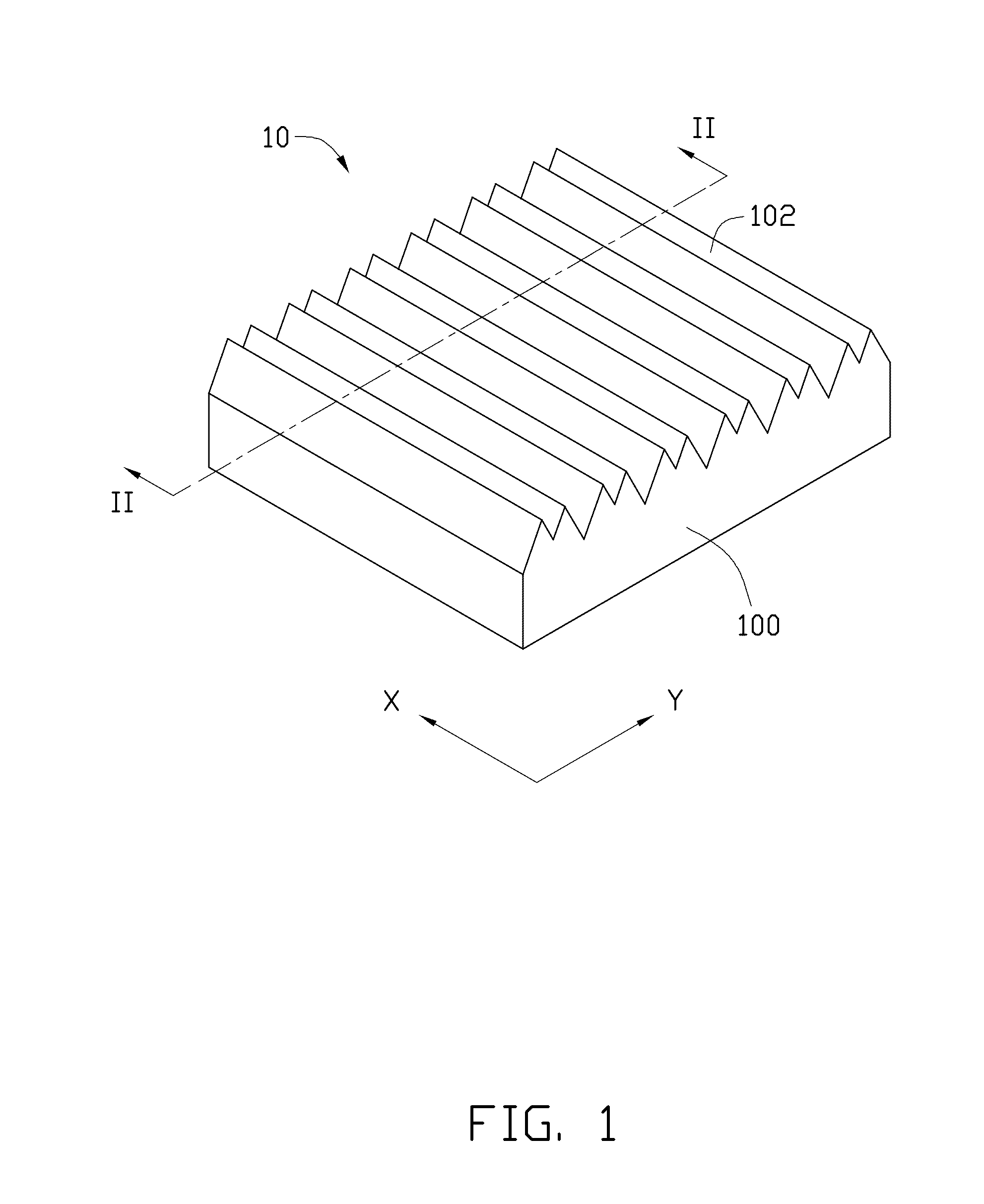
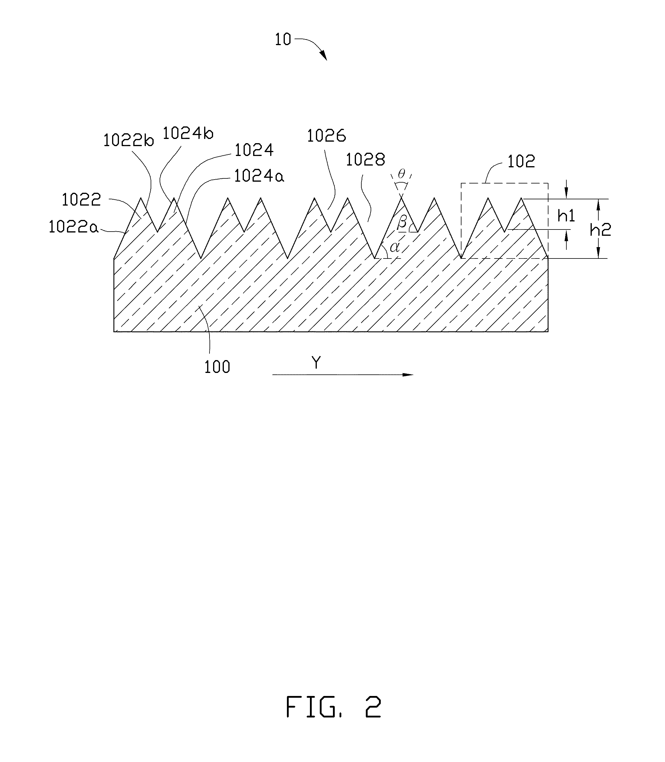
[0020]Referring to FIGS. 1 and 2, one embodiment of a three-dimensional nano-structure array 10 includes a substrate 100 and a plurality of three-dimensional nano-structures 102 located on at least one surface of the substrate 100. Each of the three-dimensional nano-structures 102 has an M-shaped cross-section. The three-dimensional nano-structure 102 having the M-shaped cross-section will be referred to as an M-shaped three-dimensional nano-structure 102 hereinafter.

[...


PUM

PropertyMeasurementUnit
poweraaaaaaaaaa
pressureaaaaaaaaaa
pressureaaaaaaaaaa

Abstract

A method for making three-dimensional nano-structure array is provided. The method includes following steps. A base is provided. A mask layer is located on the base. The mask layer is patterned, and a number of bar-shaped protruding structures is formed on a surface of the mask layer, a lot is defined between each of two adjacent protruding structures of the number of protruding structures to expose a portion of the base. The exposed portion of the base is etched through the slot so that the each of two adjacent protruding structures begin to slant face to face until they are contacting each other to form a protruding pair. The mask layer is removed.

Description

CROSS-REFERENCE TO RELATED APPLICATIONS[0001]This application claims all benefits accruing under 35 U.S.C. §119 from China Patent Application No. 201110292901.9, filed on Oct. 6, 2011 in the China Intellectual Property Office, disclosure of which is incorporated herein by reference. This application is related to applications entitled, “THREE-DIMENSIONAL NANO-STRUCTURE ARRAY”, filed Dec. 29, 2011, Ser. No. 13 / 340,194; “LIGHT EMITTING DIODE”, filed Dec. 29, 2011, Ser. No. 13 / 340,627; “METHOD FOR MAKING LIGHT EMITTING DIODE”, filed Dec. 29, 2011, Ser. No. 13 / 340,658; “LIGHT EMITTING DIODE”, filed Dec. 29, 2011, Ser. No. 13 / 340,661; “METHOD FOR MAKING LIGHT EMITTING DIODE”, filed Dec. 29, 2011, Ser. No. 13 / 340,662; “LIGHT EMITTING DIODE”, filed Dec. 29, 2011, Ser. No. 13 / 340,643.BACKGROUND[0002]1. Technical Field[0003]The present disclosure relates to a three-dimensional nano-structure array and a method for making the same.[0004]2. Description of Related Art[0005]Nano materials can be...

Claims


Application Information

Patent Timeline
Patent Type & Authority Patents(United States)
IPC IPC(8): B82Y40/00B81C1/00B29C59/14
CPCB82Y40/00B81C1/00111G03F7/0002
Inventor ZHU, ZHEN-DONGLI, QUN-QINGZHANG, LI-HUICHEN, MOJIN, YUAN-HAOFAN, SHOU-SHAN
Owner TSINGHUA UNIV
Why Eureka
Try Eureka