Thin film transistor and manufacturing method thereof

a thin film transistor and manufacturing method technology, applied in the field of flat panel displays, can solve problems such as current reduction in a channel region, and achieve the effect of increasing rc delay and increasing on curren

Active Publication Date: 2014-10-28
SAMSUNG DISPLAY CO LTD
View PDF17 Cites 4 Cited by
  • Summary
  • Abstract
  • Description
  • Claims
  • Application Information

AI Technical Summary

Benefits of technology

[0028]As described above, according to an exemplary embodiment of the present invention, a portion of the gate insulating layer corresponding to the channel region is selectively irradiated with ultraviolet rays, such that the TFT's on current may be increased without increasing RC delay.

Problems solved by technology

For this, a technique using an insulating layer having a low dielectric ratio to reduce parasitic capacitance between wires and to reduce the RC delay is applied, however, this may decrease on current in a channel region.

Method used


Image

  • Thin film transistor and manufacturing method thereof
  • Thin film transistor and manufacturing method thereof
  • Thin film transistor and manufacturing method thereof

Examples


Embodiment Construction

[0035]Exemplary embodiments of the present invention will be described in detail with reference to the accompanying drawings. However, the present invention is not limited to exemplary embodiments described herein, and may be embodied in other forms. That is, exemplary embodiments described herein are provided to thoroughly and completely understand the disclosed contents and to sufficiently transfer the ideas of the present invention to a person of ordinary skill in the art.

[0036]In drawings, the thickness of layers and regions is exaggerated for clarity. It is to be noted that when a layer is referred to as being “on” another layer or substrate, it can be directly formed on another layer or substrate or can be formed on another layer or substrate through a third layer interposed therebetween. Like constituent elements are denoted by like reference numerals throughout the specification.

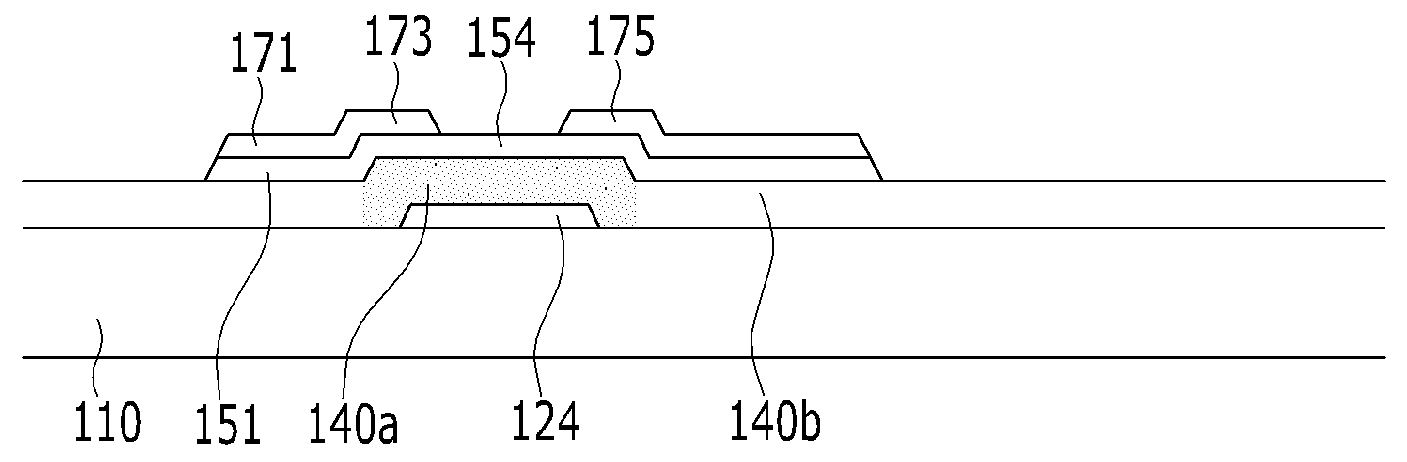
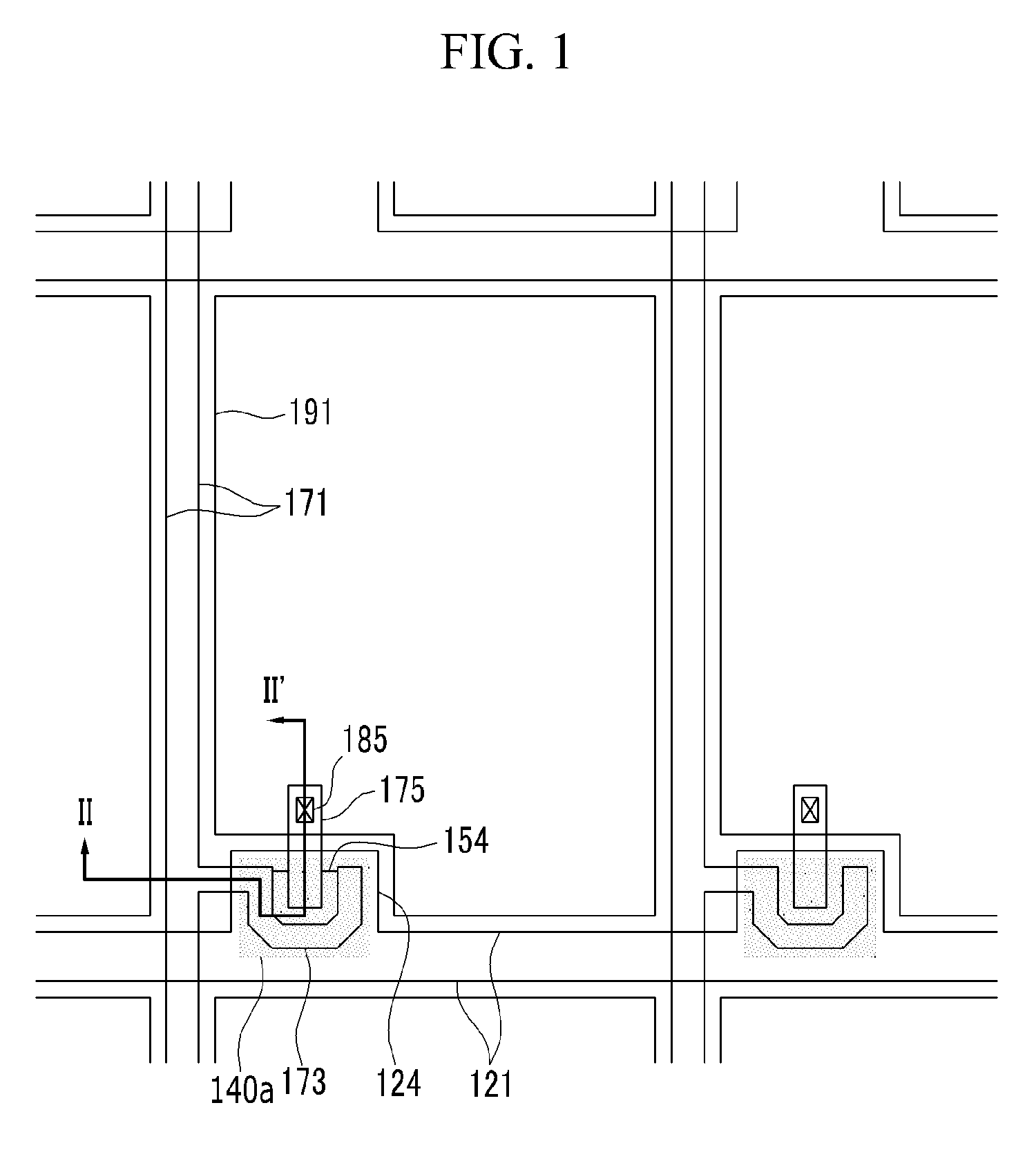
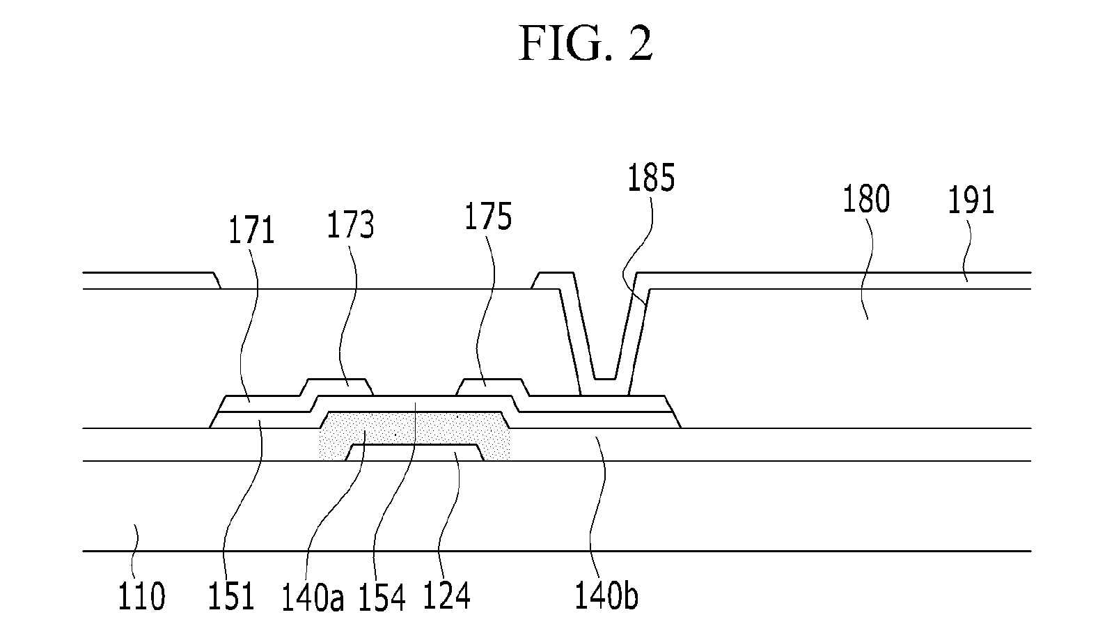
[0037]FIG. 1 is a top plan view of a thin film transistor according to an exemplary embodiment of...


PUM


Abstract

A thin film transistor is provided. A thin film transistor according to an exemplary embodiment of the present invention includes: a substrate; a gate line disposed on the substrate and including a gate electrode; a semiconductor layer disposed on the substrate and including at least a portion overlapping the gate electrode; a gate insulating layer disposed between the gate line and the semiconductor layer; and a source electrode and a drain electrode disposed on the substrate and facing each other over a channel region of the semiconductor layer. The gate insulating layer includes a first region and a second region, the first region corresponds to the channel region of the semiconductor layer, the first region is made of a first material, the second region is made of a second material, and the first material and the second material have different atomic number ratios of carbon and silicon.

Description

CROSS-REFERENCE TO RELATED APPLICATION[0001]This application claims priority to, and the benefit of, Korean Patent Application No. 10-2011-0090618 filed in the Korean Intellectual Property Office on Sep. 7, 2011, the entire contents of which are incorporated herein by reference.BACKGROUND OF THE INVENTION[0002](a) Field of the Invention[0003]Embodiments of the present invention relate generally to flat panel displays. More specifically, embodiments of the present invention relate to thin film transistors for use in flat panel displays, and manufacturing methods therefor.[0004](b) Description of the Related Art[0005]In general, thin film transistors (TFTs) are used as switching elements in an image display device or a semiconductor device.[0006]In a display device, the thin film transistor (TFT) is generally formed at an intersection of a gate wire and a data wire. The gate and data wires define unit pixel areas, and supply current for turning the unit pixel area on or off. In an on ...

Claims


Application Information

Patent Timeline
Patent Type & Authority Patents(United States)
IPC IPC(8): H01L21/00H01L29/423H01L29/49
CPCH01L29/42384H01L29/4908H01L29/786H01L29/512H01L29/51H01L2029/42388
Inventor JEONG, YEON TAEKKIM, BO SUNGLEE, DOO-HYOUNGCHOI, JUNE WHANCHOI, TAE-YOUNGMASATAKA, KANO
Owner SAMSUNG DISPLAY CO LTD
Why Eureka
Try Eureka