Method of forming damascene patterns of semiconductor devices

a technology of damascene patterns and semiconductor devices, which is applied in the details of semiconductor/solid-state devices, semiconductor devices, electrical apparatus, etc., to achieve the effects of reducing capacitance between metal lines, reducing resistance variations, and improving rc delay

Active Publication Date: 2010-07-20
SK HYNIX INC
View PDF7 Cites 0 Cited by
  • Summary
  • Abstract
  • Description
  • Claims
  • Application Information

AI Technical Summary

Benefits of technology

[0009]According to the present invention, an etch barrier layer and a second insulating layer having damascene patterns formed therein are formed over a first insulating layer in which contact plugs are formed. A mask layer is formed over the damascene patterns in which contact plugs are not formed. An etch barrier layer of regions in which the respective contact plugs are formed is then removed. Accordingly, since the damascene patterns in which the contact plugs are not formed are not exposed during an etching process, the damascene patterns can maintain a uniform depth.
[0012]According to the present invention, damascene patterns, formed in a region in which contact plugs are not formed, can have their original uniform depths. Accordingly, metal lines formed in the respective damascene patterns can have the same height and minimize a variation in the resistance according to the metal lines. Further, the metal lines formed in the respective damascene patterns of the region in which the contact plugs are not formed are formed in an insulating layer having lower capacitance than that of an etch barrier layer. Accordingly, since capacitance between the metal lines decreases and RC delay is improved, the characteristics of semiconductor devices can be improved.

Problems solved by technology

This becomes a more important issue as semiconductor devices gradually reduce in size and have higher integration.

Method used


Image

  • Method of forming damascene patterns of semiconductor devices
  • Method of forming damascene patterns of semiconductor devices
  • Method of forming damascene patterns of semiconductor devices

Examples


Embodiment Construction

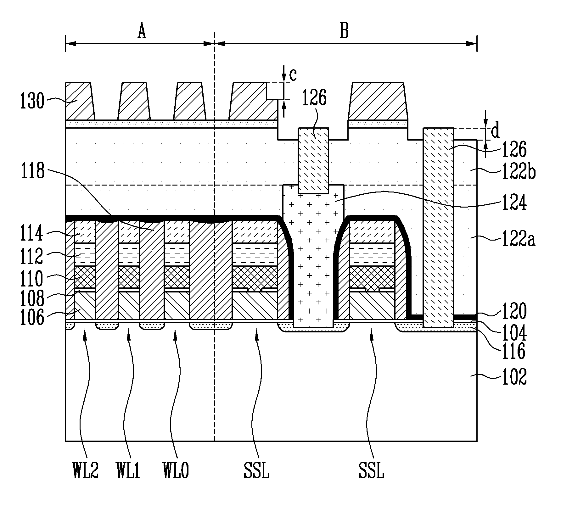
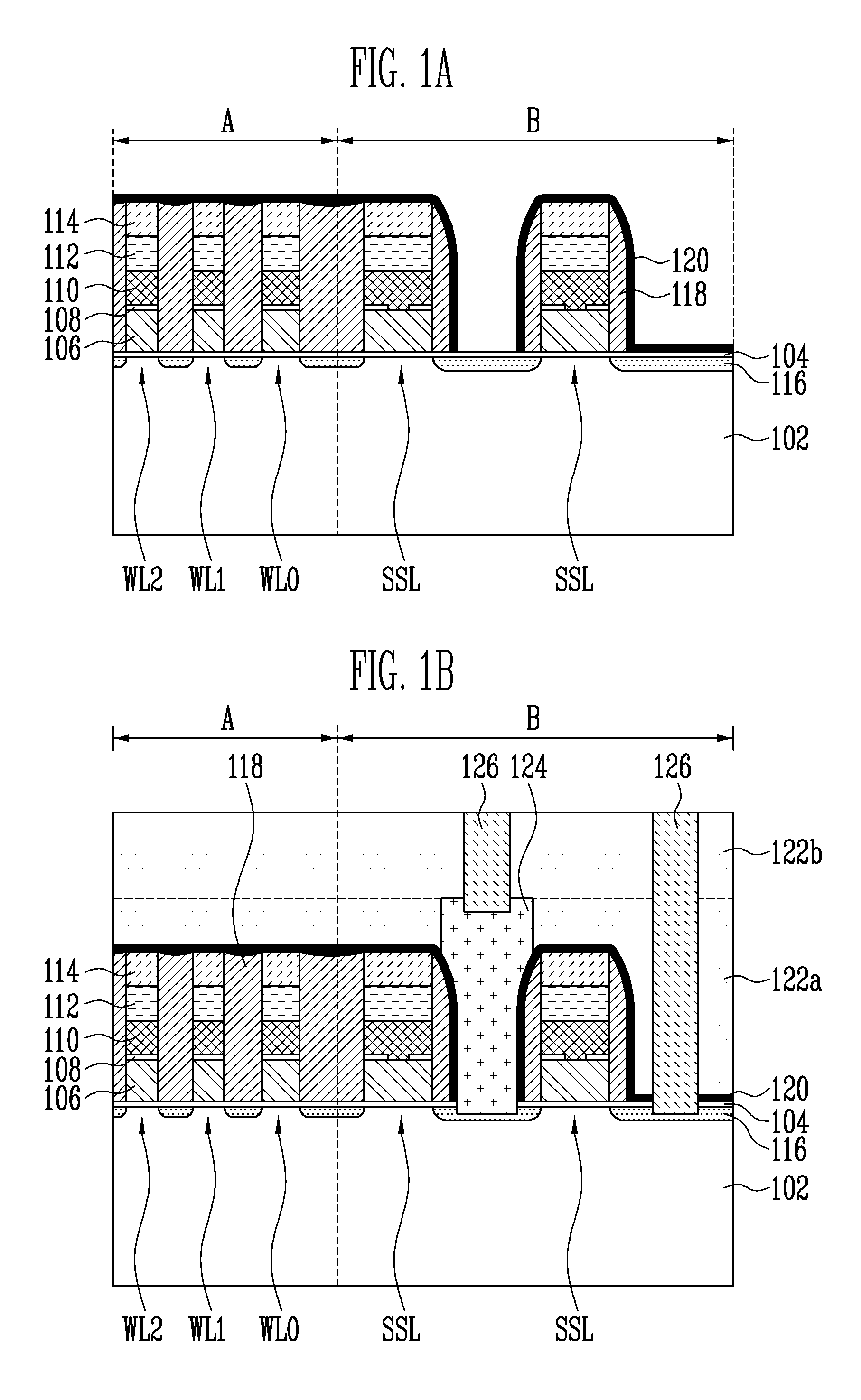
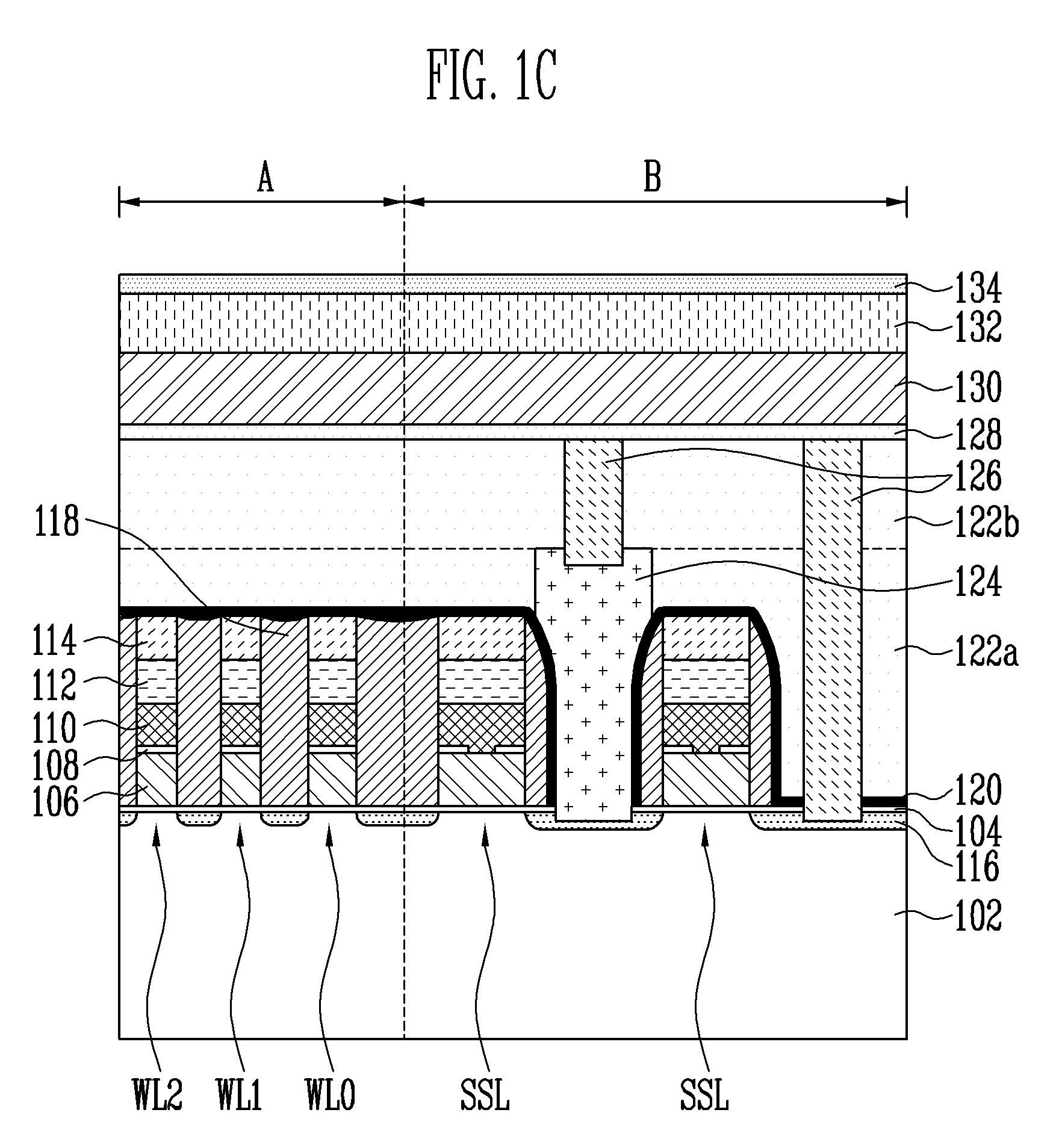
[0014]Hereinafter, the present invention will be described in detail in connection with a specific embodiment with reference to the accompanying drawings. The present embodiment is provided to complete the disclosure of the present invention and to allow those having ordinary skill in the art to understand the scope of the present invention. When it is said that any part, such as a layer, film, area, or plate, is positioned on another part, it means the part is directly on the other part or above the other part with at least one intermediate part. To clarify multiple layers and regions, the thickness of the layers is enlarged in the drawings.

[0015]FIGS. 1A to 1F are sectional views showing a method of forming damascene patterns of semiconductor devices according to the present invention.

[0016]Referring to FIG. 1A, there is provided a semiconductor substrate 102, including regions in which contact plugs are not formed (reference numeral A) and regions in which contact plugs are forme...


PUM


Abstract

A method of forming damascene patterns of semiconductor devices comprise forming a first insulating layer and contact plugs, formed in the first insulating layer, over a semiconductor substrate, forming an etch barrier layer and a second insulating layer over the first insulating layer, forming damascene patterns in the second insulating layer, forming a mask layer over the second insulating layer of other region except a region in which the contact plugs are formed so that the damascene patterns are exposed through the region in which the contact plugs are formed, removing the etch barrier layer under the exposed damascene patterns using an etching process employing the mask layer, and removing the mask layer.

Description

CROSS-REFERENCES TO RELATED APPLICATION[0001]The present application claims priority to Korean patent application number 10-2008-0006152, filed on Jan. 21, 2008, which is incorporated by reference in its entirety.BACKGROUND OF THE INVENTION[0002]The present invention relates to a method of forming damascene patterns of semiconductor devices and, more particularly, to a method of forming damascene patterns of semiconductor devices, which is capable of forming damascene patterns having a uniform depth.[0003]Semiconductor memory devices are classified into volatile memory in which data is lost when power is off and nonvolatile memory in which data can be retained although power is off.[0004]Nonvolatile memory may include Erasable Programmable Read Only Memory (EPROM), Electrically Erasable Programmable Read Only Memory (EEPROM), flash memory, and so on.[0005]Flash memory among the nonvolatile memory devices refers to devices in which data can be retained although power is off and which...

Claims


Application Information

Patent Timeline
Patent Type & Authority Patents(United States)
IPC IPC(8): H01L21/20
CPCH01L21/31144H01L21/76816H01L27/11507H01L27/11524H01L21/318H01L21/76885H10B53/30H10B41/35H01L21/28H01L21/76829
Inventor HYUN, CHAN SUN
Owner SK HYNIX INC
Why Eureka
Try Eureka