Technological method for preventing, by means of buried etch stop layers, the creation of vertical/lateral inhomogeneities when etching through-silicon vias

a technology of throughsilicon vias and etch stop layers, which is applied in the direction of semiconductor devices, semiconductor/solid-state device details, electrical devices, etc., can solve the problems of limited width and depth of the etching process

Active Publication Date: 2018-10-04
IHP GMBH INNOVATIONS FOR HIGH PERFORMANCE MICROELECTRONICS LEIBNIZ INST FUR INNOVATIVE
View PDF6 Cites 5 Cited by
  • Summary
  • Abstract
  • Description
  • Claims
  • Application Information

AI Technical Summary

Benefits of technology

[0030]In one preferred variant of the method, the etch stop layer comprises an insulating material such as SiO2. This allows the etch stop layer to be used as an insulating layer between the silicon wafer and the metallization layer after the TSVs have been exposed. In this way, the additional step of depositing an insulating layer can be avoided.
[0031]In another variant, the silicon wafer and / or the first carrier wafer is thinned before the active components are produced. This is advantageous for setting desired wafer thicknesses independently of the standardized thicknesses of the initial wafers, i.e., of the unprocessed silicon wafer or the first carrier wafer. It is advantageous, more particularly, if the silicon wafer is set to a final thickness for the semiconductor device by thinning the silicon wafer. This obviates the need for subsequent thinning in steps in which other components are already implemented in or on the wafer and would be adversely affected by the thinning process.

Problems solved by technology

This means that the etching process is defined and limited not only in depth, but also in width, by the previously implemented structure of the etch stop layer resulting from the original raised portions.

Method used


Image

  • Technological method for preventing, by means of buried etch stop layers, the creation of vertical/lateral inhomogeneities when etching through-silicon vias
  • Technological method for preventing, by means of buried etch stop layers, the creation of vertical/lateral inhomogeneities when etching through-silicon vias
  • Technological method for preventing, by means of buried etch stop layers, the creation of vertical/lateral inhomogeneities when etching through-silicon vias

Examples


Embodiment Construction

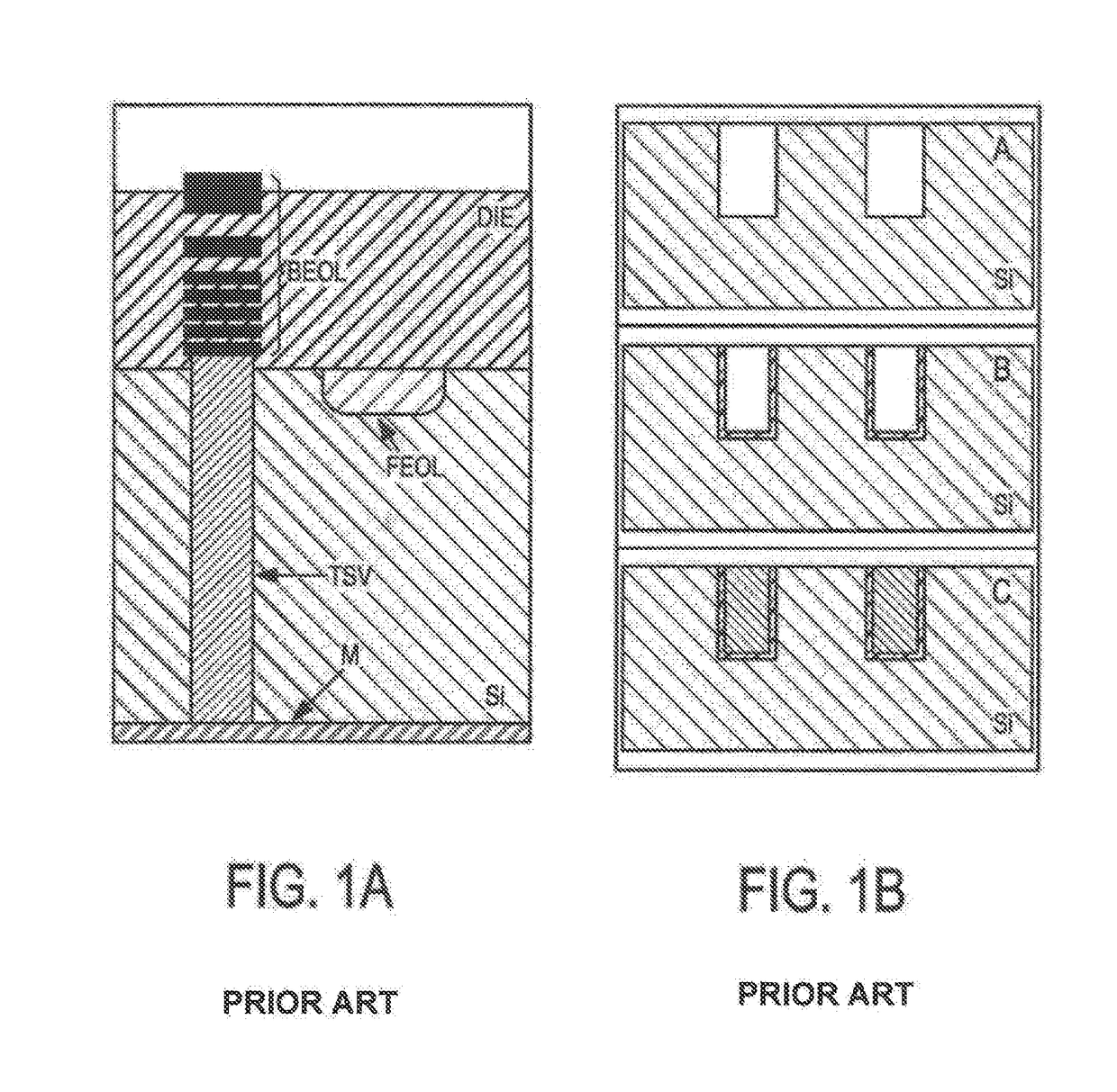
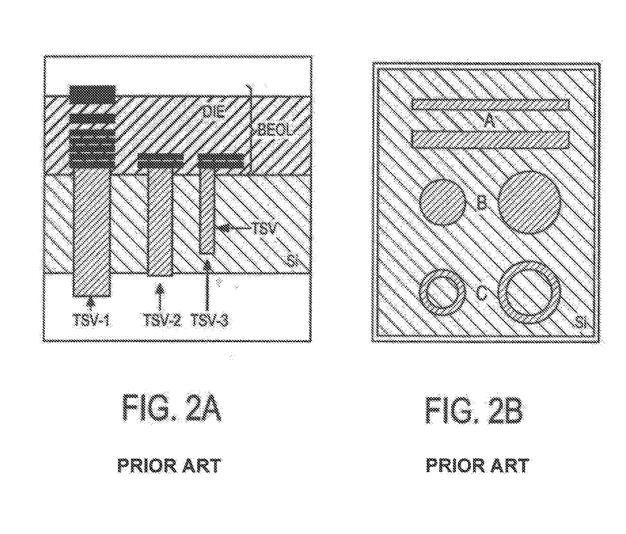
[0044]Reference has already been made to FIGS. 1A to 2B in the introductory section above.

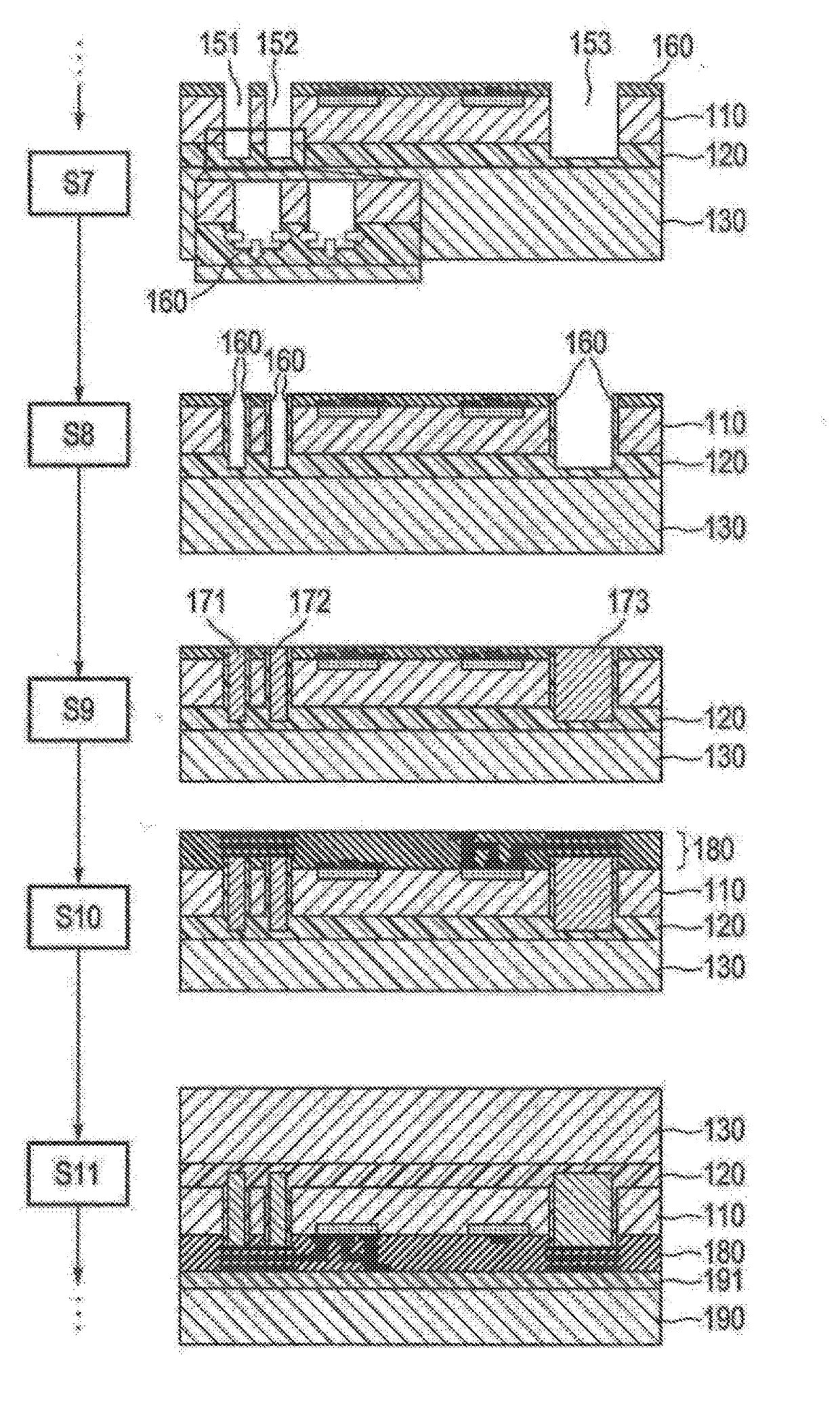
[0045]FIGS. 3A to 3C show a method for producing a semiconductor device 100 according to the first aspect of the invention. In step S1, a silicon wafer 110 having a plurality of raised portions 101, 102, 103 of equal height h are provided on a first surface 111 of silicon wafer 110. In the further course of the method, raised portions 101, 102, 103 serve as placeholders for through-silicon vias. The cross-sectional geometry of the raised portions is substantially the same as the cross-sectional geometry of the through-silicon vias that ensue. As can be seen clearly in FIG. 3A, the thicknesses of raised portions 101 and 103 differ significantly. In the embodiment shown here, raised portions 101, 102, 103 were produced on an unprocessed silicon wafer by silicon etching. In step S2, an etch stop layer 120 is deposited on the first surface 111 of silicon wafer 110. Etch stop layer 120 is made here ...


PUM


Abstract

Method for producing a semiconductor device by providing a silicon wafer having a plurality of equal height raised portions on a first surface thereof; depositing an etch stop layer on the first surface; planarizing a surface of the etch stop layer; permanently bonding a first carrier wafer on the etch stop layer surface; producing components on or in a second wafer surface in a FEOL process; etching a plurality of trenches into the wafer, each trench formed at the respective location of one of the raised portions; depositing side wall insulation layers on side walls of the trenches; forming through-silicon vias by filling the trenches with electrically conductive material; producing a conductor path stack in a BEOL process for contacting the active components on the second surface; temporarily bonding a second carrier wafer onto a surface of the conductor path stack; removing the first carrier wafer and exposing the vias.

Description

CROSS REFERENCE TO RELATED APPLICATION[0001]This application claims priority under 35 USC § 119 to German Patent Application No. 10 2016 219 275.2 filed on Oct. 5, 2016, which application is hereby incorporated by reference in its entirety.TECHNICAL FIELD[0002]The invention relates to a method for producing semiconductor devices, in particular wafers having through-silicon vias (TSVs).BACKGROUND OF THE INVENTION[0003]The integration of vertical vias through the silicon substrate, that is to say through-silicon vias, is a technique that is used, for example, for high-frequency grounding in low-noise amplifiers (LNAs) and power amplifiers (PAs), as well as for signal transfer for three-dimensionally stacked CMOS / BiCMOS chips. The basic architecture of a silicon (Si)-based chip with TSVs is shown in FIG. 1A. The back-end-of-line (BEOL) conductor path stack arranged in a dielectric (DiE) is conductively connected, through the silicon substrate (Si), by a through-silicon via (TSV) to bac...

Claims


Application Information

Patent Timeline
Patent Type & Authority Applications(United States)
IPC IPC(8): H01L21/768H01L21/683H01L21/306H01L21/78H01L23/48H01L23/528H01L21/308H01L23/66
CPCH01L21/76898H01L21/6835H01L21/30604H01L21/78H01L23/481H01L23/528H01L21/3086H01L23/66H01L2221/68359H01L2223/6616
Inventor WIETSTRUCK, MATTHIASKAYNAK, MEHMETKULSE, PHILIPLISKER, MARCOMARSCHMEYER, STEFFENWOLANSKY, DIRK
Owner IHP GMBH INNOVATIONS FOR HIGH PERFORMANCE MICROELECTRONICS LEIBNIZ INST FUR INNOVATIVE
Why Eureka
Try Eureka