Threshold voltage modulation image sensor

a technology of threshold voltage and image sensor, which is applied in the field of threshold voltage (vth) modulation image sensor, can solve the problems of complex pixel structure of ccd image sensor, difficult to integrate ccd image sensor in the same chip as that of peripheral signal processing circuit, and require a process, so as to achieve the effect of increasing light sensitivity and miniaturizing the pixel region

Inactive Publication Date: 2010-03-23
FUJITSU SEMICON LTD
View PDF19 Cites 5 Cited by
  • Summary
  • Abstract
  • Description
  • Claims
  • Application Information

AI Technical Summary

Benefits of technology

[0008]Further, in the Vth modulation image sensor, the potential pocket for increasing the sensitivity is established close to the source region in the ring and spaced apart from the drain region. By spacing the potential pocket apart from the drain region, the junction capacity with the drain region is reduced, the variation in the threshold value of the potential pocket region is increased given even a small amount of electrical charge, and the sensitivity is raised.
[0019]According to aspects 1 to 5 of the present invention above, the potential pocket region can be provided below the gate electrode without shifting to the source-region side and the gate electrode width can be narrowed, whereby the pixel region can be miniaturized. Further, the depth of the potential of the potential pocket region can be made substantially uniform and the light sensitivity can be raised.
[0020]In addition, according to aspects 6 and 7 of the present invention above, as a result of the provision of a miniaturized pixel region, the problem posed by a structure in which electrical charge accumulated in the well region due to the fluctuation of the gate voltage is readily released to the substrate side can be avoided.

Problems solved by technology

However, CCD image sensors have a complex pixel structure and require a process that is different from an ordinary CMOS process.
It is therefore not easy to incorporate a CCD image sensor in the same chip as that of a peripheral signal processing circuit.
A general CMOS image sensor comprises, in a single pixel, a plurality of transistors and a photoelectric conversion element such as a photodiode, and hence miniaturization of the pixel size is difficult.

Method used


Image

  • Threshold voltage modulation image sensor
  • Threshold voltage modulation image sensor
  • Threshold voltage modulation image sensor

Examples


first embodiment

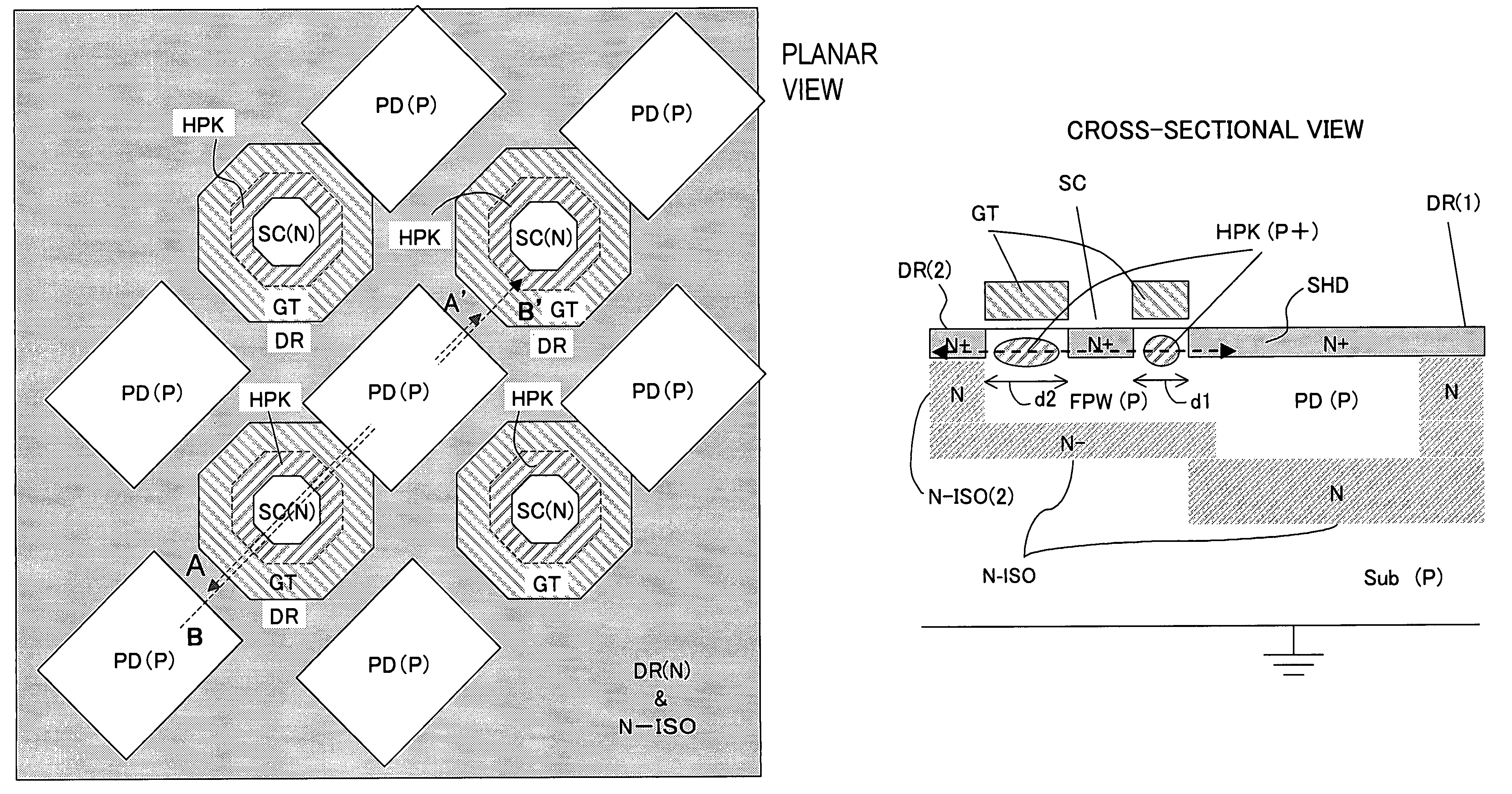
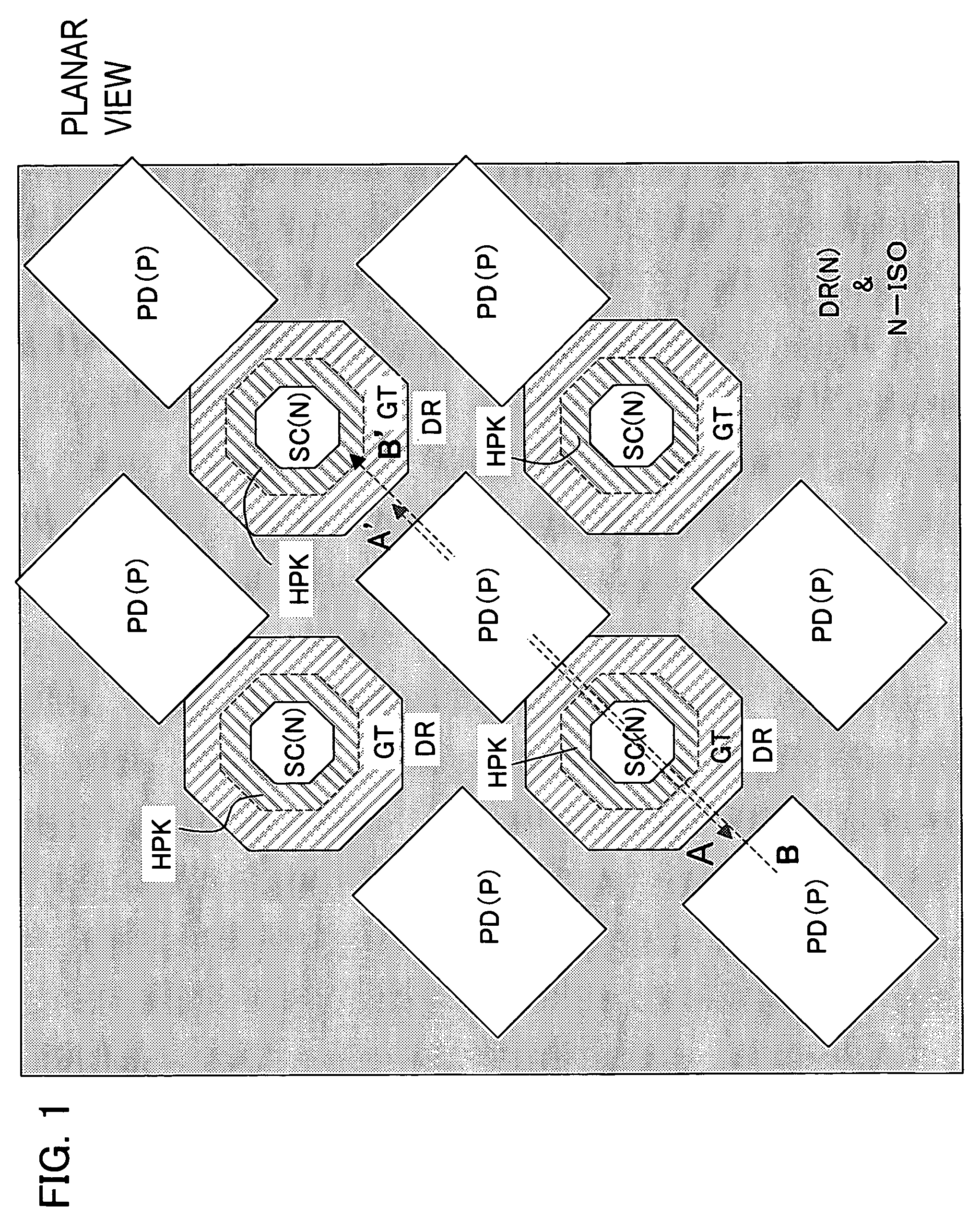
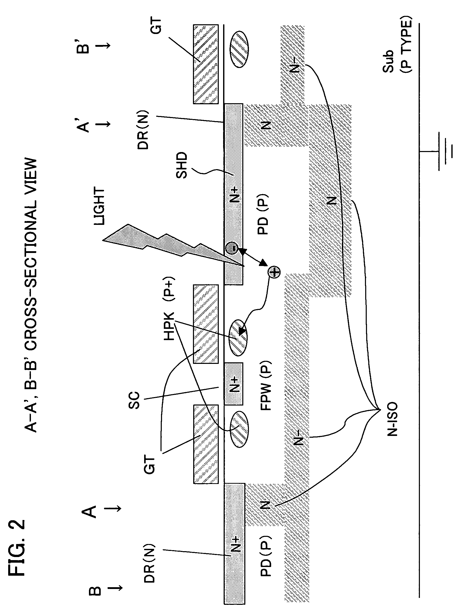
[0064]FIG. 5 shows a cross-sectional view and a hole potential diagram of an image sensor of a The planar shape of the image sensor of this embodiment is as per FIG. 3A, but, this planar shape is different in that the width of the gate electrode GT is narrower on the side of the photoelectric conversion region PD. That is, as illustrated by the cross-sectional view in FIG. 5A, the gate width of the gate electrode GT is narrower in part d1 close to the photoelectric conversion region PD than in part d2 outside the photoelectric conversion region PD. Further, a high-density P-type potential pocket region HPK is formed over the whole surface of the floating P-type well region FPW below the gate electrode GT. For this reason, the width d1 of the PD-side potential pocket region HPK(PD) is then narrower than the width d2 of the potential pocket region HPK(Non-PD) on the side of the N-type isolation region N-ISO (2) in the substrate. However, because the potential pocket region HPK is not...

second embodiment

[0066]FIG. 6 provides a cross-sectional view and a hole potential diagram of the image sensor of the In this example, the widths d1 and d2 of the ring-like gate electrode GT are substantially constant or equal and the width of the potential pocket region HPK is substantially constant or equal. However, the P-type impurity concentration of the PD-side potential pocket region HPK (P+) is made lower than the P-type impurity concentration of the potential pocket region HPK (P++) that is adjacent to the N-type isolation region N-ISO(2) in the substrate outside the PD region. As per the planar and cross-sectional views, the pocket region HPK is such that the PD-side region is P+ (high-density P-type region) and the remaining region is P++ (a higher density P-type region). Thus, by providing such a difference in density, the potential depth of the PD-side pocket region can be made shallow and the potential non-uniformity with respect to the pocket region HPK close to the isolation region ...

third embodiment

[0068]FIG. 7 provides a cross-sectional view and a hole potential diagram of the image sensor of the So too with this example, the widths d1 and d2 of the ring-like gate electrode GT are substantially constant and the width of the potential pocket region HPK is substantially constant. In addition, the impurity concentration is also substantially constant. However, an offset structure OFFSET that spaces the N-type isolation region N-ISO provided in the substrate apart from the gate electrode near the gate electrode GT is provided. That is, the planar view of FIG. 7A illustrates the relationship between the N-type isolation region N-ISO formed in the substrate and the gate electrode GT and photoelectric conversion region PD. However, the N-type isolation region N-ISO is formed with an offset OFFSET in the region of the gate electrode GT that is not adjacent to the photodiode PD. That is, as indicated by the arrow 10 in the cross-sectional view of FIG. 7B, the N-type isolation region ...


PUM


Abstract

An image sensor has a plurality of pixels each with a photoelectric conversion element and a detection transistor the threshold voltage of which fluctuates in accordance with electrical charge generated in the photoelectric conversion element. The image sensor includes a second conductivity type shield region and a first conductivity type photoelectric conversion region; a first conductivity type well region linked to the photoelectric conversion region; a ring-like gate electrode; a second conductivity type source region at the inside of the ring-like gate electrode; a second conductivity type drain region. The image sensor further includes a potential pocket region that is formed in the well region below the ring-like gate electrode and accumulates the electrical charge, wherein the width of the gate electrode is formed narrower in the part adjacent to the photoelectric conversion region than in other parts.

Description

CROSS-REFERENCE TO RELATED APPLICATIONS[0001]This application is based upon and claims the benefit of priority from the prior Japanese Patent Application No. 2004-190853, filed on Jun. 29, 2004, the entire contents of which are incorporated herein by reference.BACKGROUND OF THE INVENTION[0002]1. Field of the Invention[0003]The present invention relates to a threshold voltage (Vth) modulation image sensor and, more particularly, to a Vth modulation image sensor that permits pixel miniaturization.[0004]2. Description of the Related Art[0005]Image sensors that employ CCD are widely used. However, CCD image sensors have a complex pixel structure and require a process that is different from an ordinary CMOS process. It is therefore not easy to incorporate a CCD image sensor in the same chip as that of a peripheral signal processing circuit. On the other hand, as an image sensor that can be fabricated by means of a CMOS process, a CMOS image sensor has been proposed. A general CMOS image ...

Claims


Application Information

Patent Timeline
Patent Type & Authority Patents(United States)
IPC IPC(8): H01L27/146H01L31/062H04N5/335H04N5/369H04N5/374
CPCH01L27/14603H01L27/14609H01L27/1463H01L27/14689H01L21/8238H01L27/146H01L31/10
Inventor OHKAWA, NARUMIASANO, MASAYOSHINOMURA, TOSHIO
Owner FUJITSU SEMICON LTD
Why Eureka
Try Eureka