Method for fabricating low-k dielectric and Cu interconnect

a dielectric and cu interconnection technology, applied in the field of integrated circuits, can solve the problems of achieve the effects of less carbon depletion, increasing the rc delay of the integrated circuit produced and raising the capacitan

a dielectric and cu interconnection technology, applied in the field of integrated circuits, can solve the problems of achieve the effects of less carbon depletion, increasing the rc delay of the integrated circuit produced and raising the capacitan

US7998873B2Inactive Publication Date: 2011-08-16TAIWAN SEMICON MFG CO LTD

Image

  • Method for fabricating low-k dielectric and Cu interconnect
  • Method for fabricating low-k dielectric and Cu interconnect
  • Method for fabricating low-k dielectric and Cu interconnect

Examples


Embodiment Construction

[0019]The making and using of the presently preferred embodiments are discussed in detail below. It should be appreciated, however, that the present invention provides many applicable inventive concepts that can be embodied in a wide variety of specific contexts. The specific embodiments discussed are merely illustrative of specific ways to make and use the invention, and do not limit the scope of the invention.

[0020]The present invention will be described with respect to preferred embodiments in a specific context, namely a dual damascene etch process. The invention may also be applied, however, to other low-k etch processes.

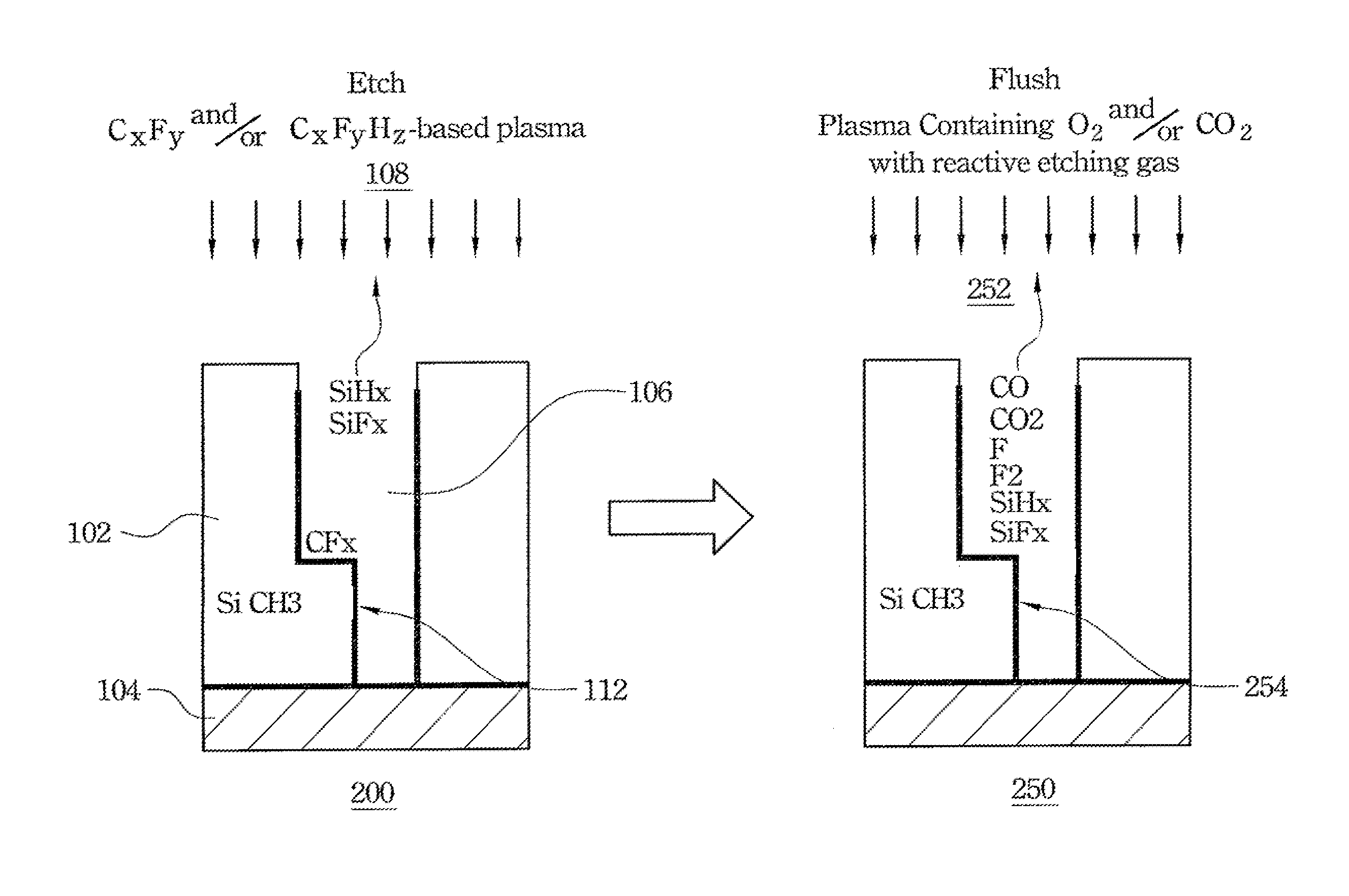
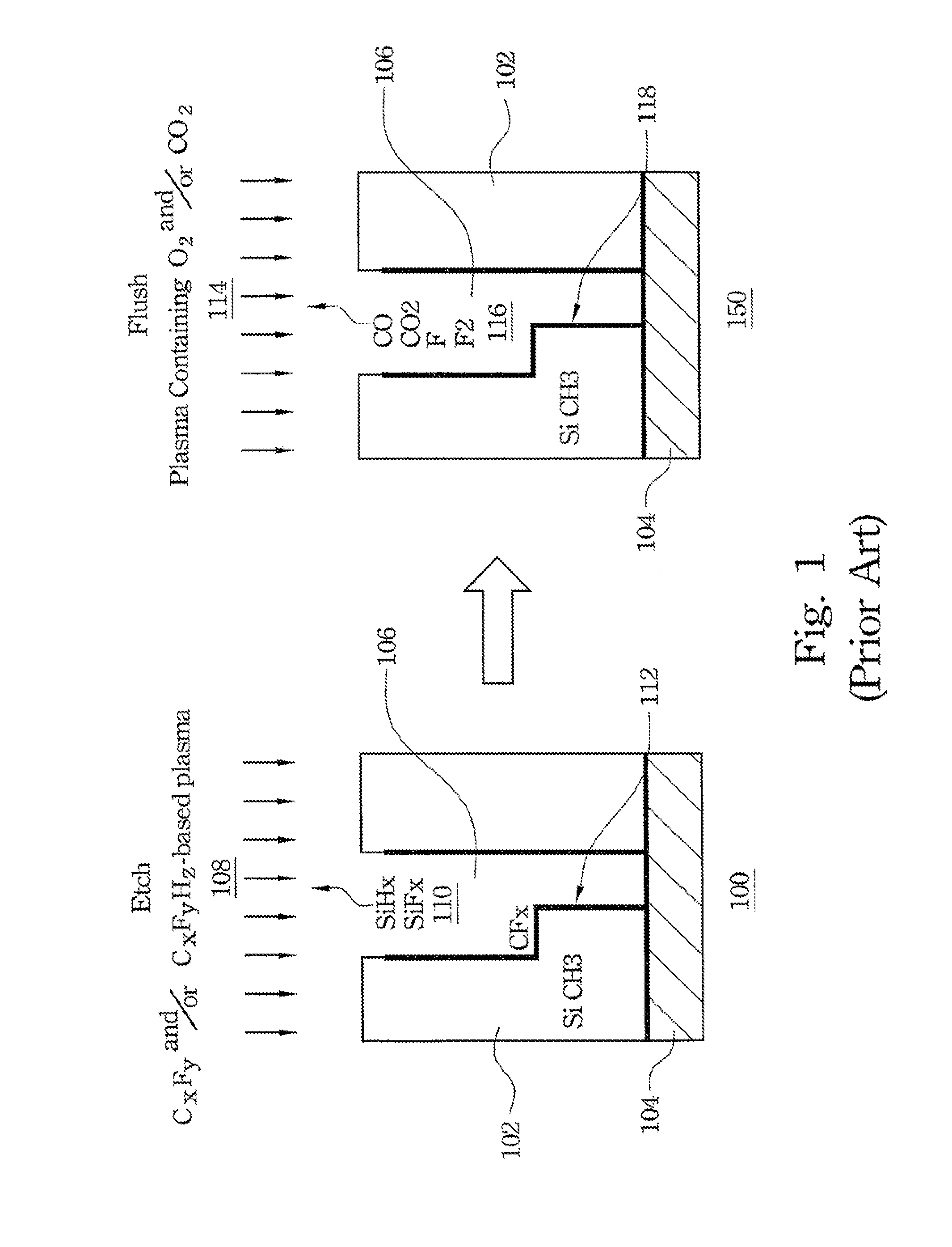
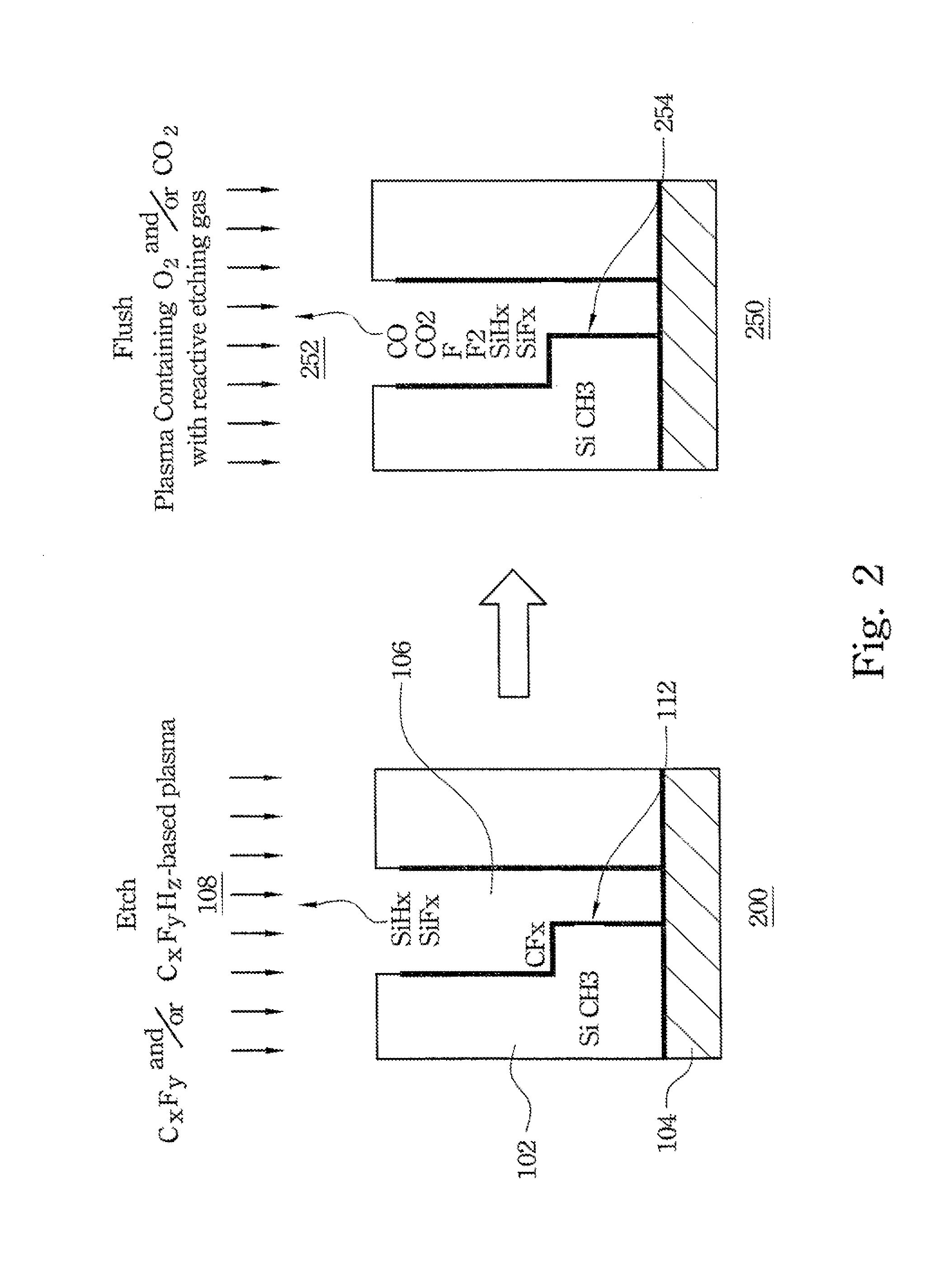
[0021]With reference now to FIG. 1, shown are two cross sectional drawings of an etch region of a low-k dielectric of a known dual damascene process. Post etch drawing 100 shows low-k dielectric layer 102 on metal layer 104 following etch. The dual damascene etch has been performed, leaving opening 106 in low-k dielectric layer 102. Reactive etch gases CxFyHz a...


PUM


Abstract

A system and method for improving the performance of an integrated circuit by lowering RC delay time is provided. A preferred embodiment comprises adding a reactive etch gas to the ash / flush plasma process following a low-k dielectric etch. The illustrative embodiments implement a removal of the damage layer that is formed during a low-k dielectric etch.

Description

TECHNICAL FIELD[0001]The present invention relates generally to integrated circuits, and more particularly to a system and method for minimizing damage caused by a low-k dielectric etch process.BACKGROUND[0002]In semiconductor manufacturing, a low-k dielectric is a material with a small dielectric constant relative to silicon dioxide. Silicon dioxide has a k value of 3.9. Materials with k values less than 3.9 are considered low-k dielectric materials. In digital circuits, insulating dielectrics separate interconnects and transistors from one another. As integrated circuits have minimized, components have scaled correspondingly and the insulating dielectrics have thinned to the point where charge build up and crosstalk adversely affect the performance of the circuit. Replacing the silicon dioxide with a low-k dielectric reduces parasitic capacitance, enabling faster switching speeds and lower heat dissipation.[0003]Dual damascene processing is a method for fabricating planar intercon...

Claims


Application Information

Patent Timeline
16 Aug 2011
Publication
US7998873B2
IPC
H01L21/302; H01L21/461
CPC
H01L21/02063; H01L21/31138; H01L21/76814
Inventors
CHEN, CHIH-HAO; CHOU, CHIA-CHENG