Barrier layer for interconnection structure and preparation method thereof

A technology of interconnection structure and barrier layer, applied in semiconductor/solid-state device manufacturing, electrical components, electric solid-state devices, etc., can solve the problems of unsatisfactory barrier layer effect, etc., to improve poor performance, improve RC delay, and reduce heat Effect

Pending Publication Date: 2021-11-19
广东汉岂工业技术研发有限公司
View PDF0 Cites 0 Cited by
  • Summary
  • Abstract
  • Description
  • Claims
  • Application Information

AI Technical Summary

Problems solved by technology

However, the quality of the TaN barrier layer deposited by the ALD method is not as good as that of the TaN barrier layer deposited by the PVD method, therefore, the effect of depositing a TaN thin film barrier layer on the interconnect line by ALD method alone is not ideal

Method used


Image

  • Barrier layer for interconnection structure and preparation method thereof
  • Barrier layer for interconnection structure and preparation method thereof

Examples


Embodiment 1

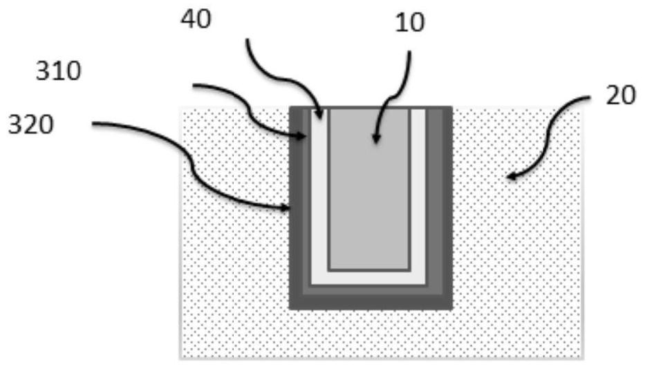
[0026] In order to solve the foregoing technical problems, the present invention provides a barrier layer for an interconnection structure, which is disposed between the metal interconnection material 10 and the dielectric layer 20 of the interconnection structure, and the barrier layer includes a first barrier layer 310 and a second barrier layer 320 , the first barrier layer 310 surrounds the outer layer of the metal interconnection material 10 , and the second barrier layer 320 surrounds the first barrier layer 310 outside. Wherein, the first barrier layer and the second barrier layer are formed by atomic layer deposition.

[0027] Specifically, in an embodiment of the present invention, the materials of the first barrier layer and the second barrier layer are different. The first barrier layer is made of a material with stable metal properties and good adhesion, so as to improve the adhesion between the second barrier layer and the metal interconnection material. Further,...

Embodiment 2

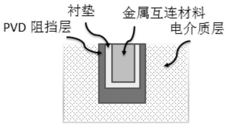
[0030] Such as figure 1 As shown, the present invention provides an interconnection structure comprising a metal interconnection material 10 , a dielectric layer 20 , a barrier layer and a liner 40 . Wherein, the liner 40 is disposed outside the metal interconnection material 10 , and the barrier layer is disposed between the liner 40 and the dielectric layer 10 . The barrier layer includes a first barrier layer 310 disposed on the outer layer of the liner 40 and a second barrier layer 320 disposed outside the first barrier layer. Wherein, the metal interconnection material is Cu.

Embodiment 3

[0032] The present invention provides a method for preparing a barrier layer for an interconnect structure, comprising the steps of:

[0033] depositing a first barrier layer outside the metal interconnect material of the interconnect structure;

[0034] A second barrier layer is deposited outside the first barrier layer.

[0035] Specifically, in an embodiment of the present invention, the first barrier layer and the second barrier layer are formed by atomic layer deposition. Since the two barrier layers are deposited by atomic layer deposition, the two barrier layers can be formed at the same temperature through one ALD chamber, thereby improving production efficiency.

[0036] The present invention also provides an electronic device comprising an interconnection structure manufactured according to the method of an exemplary embodiment of the present invention. The electronic device can be any electronic product or equipment such as a mobile phone, a tablet computer, a not...


PUM


Abstract

The invention discloses a barrier layer for an interconnection structure. The barrier layer is arranged between a metal interconnection material and a dielectric layer of an interconnection structure, and comprises a first barrier layer and a second barrier layer, wherein the first barrier layer surrounds the outer layer of the metal interconnection material, and the second barrier layer surrounds the outer side of the first barrier layer. The barrier layer provided by the invention comprises the two barrier layers formed by atomic layer precipitation, the two barrier layers are made of different materials, and the adhesive force between the original barrier layer and the metal interconnection material can be improved by utilizing the material with stable metal performance and good adhesive force, so that the problems that an existing single barrier layer is poor in performance and high impedance is caused by double barrier layers formed by ALD and PVD can be solved so as to reduce the heat from the interconnection current to the damage of the integrated circuit, improve the RC delay of the IC circuit is improved and improve the yield of IC production.

Description

technical field [0001] The invention relates to the technical field of semiconductors, in particular to a barrier layer for an interconnection structure, a preparation method and an interconnection structure comprising the barrier layer. Background technique [0002] When making semiconductor integrated circuits, it is usually necessary to make metal interconnection structures for electrically connecting semiconductor devices. The metal interconnection structure is usually made in an insulating material layer, which requires manufacturing a trench (trench) or a connecting hole on the insulating material layer, and then depositing metal in the trench or connecting hole, the deposited metal is It is a metal interconnection wire, and copper is generally selected as the metal interconnection wire material. [0003] When metal copper is selected as the metal interconnect material, a metal barrier layer is usually deposited between the metal interconnect material and the insulati...

Claims


Application Information

Patent Timeline
Patent Type & Authority Applications(China)
IPC IPC(8): H01L23/532H01L21/768
CPCH01L23/53238H01L21/76846
Inventor 杨弦龙姜德新
Owner 广东汉岂工业技术研发有限公司
Why Eureka
Try Eureka