Fin field-effect transistors and fabrication method thereof

a technology of field-effect transistors and fabrication methods, which is applied in the direction of basic electric elements, semiconductor devices, electrical equipment, etc., can solve the problems of reducing the critical dimension (cd), unable to meet the requirements of device performance, and difficult to use such a method to adjust the threshold voltage of the fin

Active Publication Date: 2014-11-11
SEMICON MFG INT (SHANGHAI) CORP
View PDF1 Cites 32 Cited by
  • Summary
  • Abstract
  • Description
  • Claims
  • Application Information

AI Technical Summary

Benefits of technology

[0006]One aspect of the present disclosure includes a method for fabricating a fin field-effect transistor. The method includes providing a semiconductor substrate having one or more first fins and second fins; and forming a first doping layer covering the first fins and the second fins. The method also includes forming an isolation layer to isolate adjacent fins; and forming a gate structure stretch across top and sidewalls of the first f

Problems solved by technology

However, when the critical dimension (CD) is further reduced, the structures of conventional MOS field effect transistors (MOSFETs) are unable to match requirements of

Method used


Image

  • Fin field-effect transistors and fabrication method thereof
  • Fin field-effect transistors and fabrication method thereof
  • Fin field-effect transistors and fabrication method thereof

Examples


Embodiment Construction

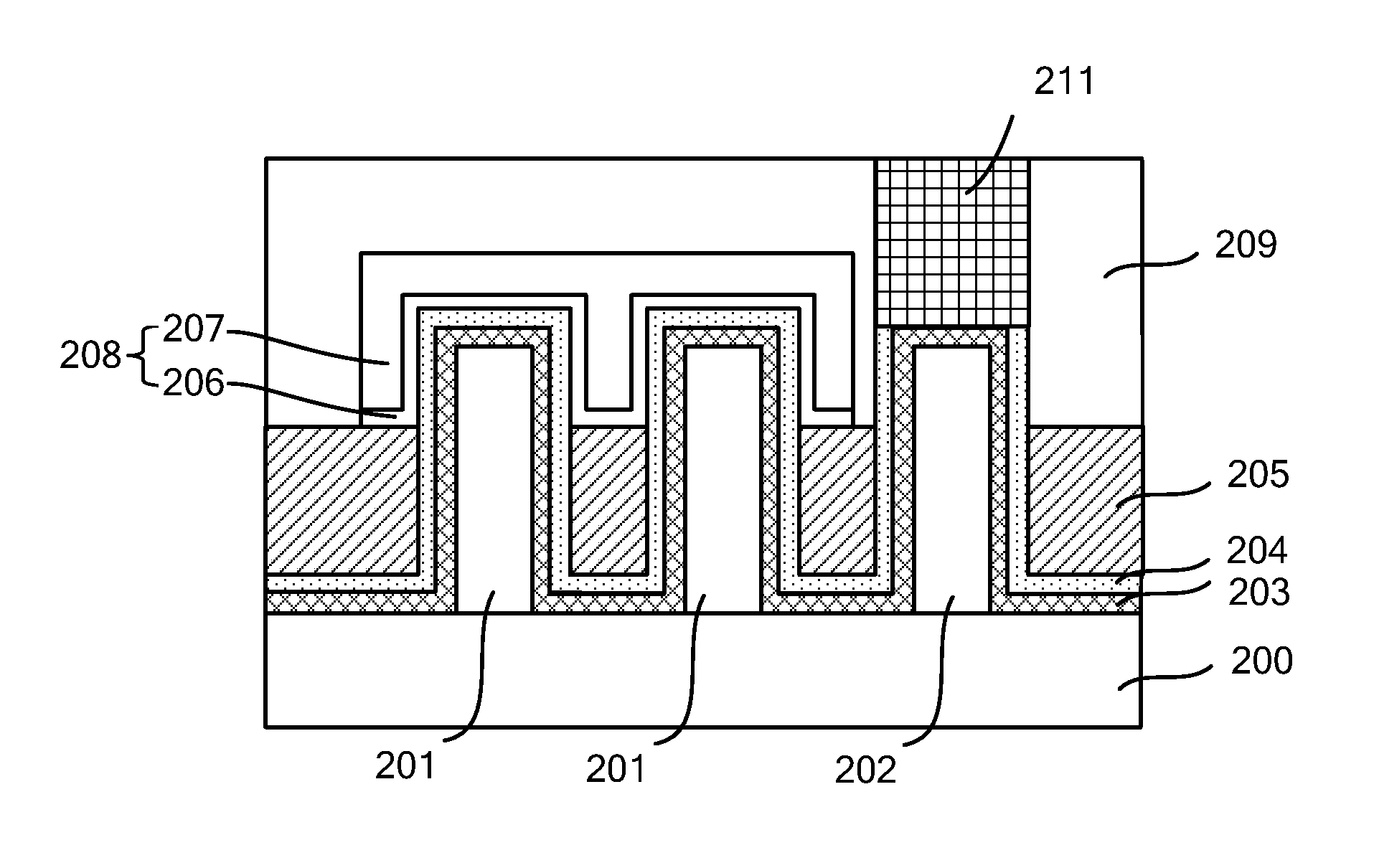
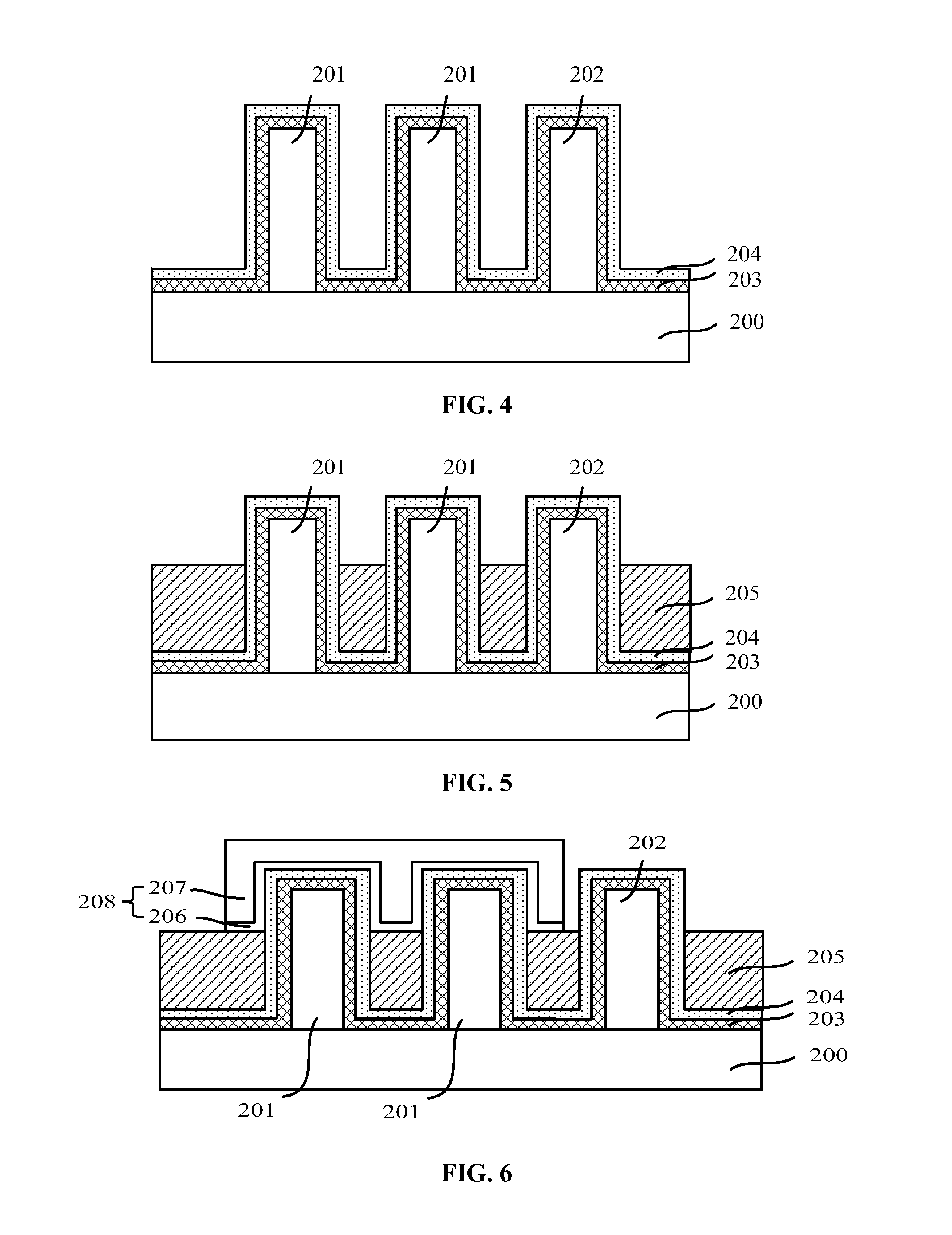
[0012]Reference will now be made in detail to exemplary embodiments of the invention, which are illustrated in the accompanying drawings. Wherever possible, the same reference numbers will be used throughout the drawings to refer to the same or like parts.

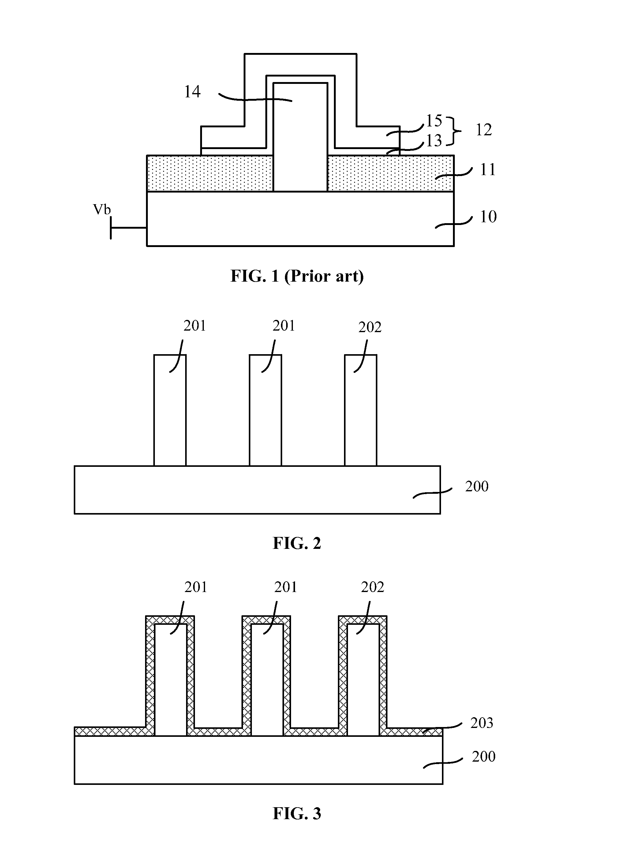
[0013]Referring to FIG. 1, when the threshold voltage of the FinFET is adjusted, the substrate 10 may often be connected with a bias voltage Vb. The bias voltage Vb may need to go through the semiconductor substrate 10 and the fin 14 to transfer to a vicinity of the surface of the fin 14 on the bottom of the gate structure 12, thus a transfer path of the bias voltage Vb may be significantly long; and a resistance of along the transfer path may be relatively large. Therefore, the potential on the surface of the fin 14 on the bottom of the gate structure 12 applied by the bias voltage Vb may be substantially small. The small potential may adverse to adjusting the threshold voltage of the FinFET; and the bias voltage Vb may have a rel...


PUM


Abstract

A method is provided for fabricating a fin field-effect transistor. The method includes providing a semiconductor substrate having one or more first fins and second fins; and forming a first doping layer covering the first fins and the second fins. The method also includes forming an isolation layer to isolate adjacent fins; and forming a gate structure stretching across top and sidewalls of the first fins. Further, the method includes forming a source region and a drain region in the fins at both sides of the gate structure; and forming a dielectric layer on the isolation layer. Further, the method also includes forming a first through hole in the dielectric layer to expose a portion of the first doping layer on a top of the second fins; and forming a first conductive via in the first through hole to connect with a bias control voltage.

Description

CROSS-REFERENCES TO RELATED APPLICATIONS[0001]This application claims the priority of Chinese patent application No. 201310259904.1, filed on Jun. 26, 2013, the entirety of which is incorporated herein by reference.FIELD OF THE INVENTION[0002]The present invention generally relates to the field of semiconductor manufacturing technology and, more particularly, relates to fin field-effect transistors and fabrication techniques thereof.BACKGROUND[0003]With the development of the semiconductor manufacturing technology, technical nodes have consistently decreased, thus a gate-last process has been widely used to obtain an ideal threshold voltage to improve the device performance. However, when the critical dimension (CD) is further reduced, the structures of conventional MOS field effect transistors (MOSFETs) are unable to match requirements of the device performance even the gate-last process is used to form MOSFETs. Fin field-effect transistors (FinFET) have attracted extensive attenti...

Claims


Application Information

Patent Timeline
IPC IPC(8): H01L21/336H01L29/78H01L29/66
CPCH01L29/66795H01L29/785H01L21/823431H01L29/6681H01L21/845
Inventor FUMITAKE, MIENO
Owner SEMICON MFG INT (SHANGHAI) CORP
Why Eureka
Try Eureka