System and method for integrated circuits with cylindrical gate structures

a technology of integrated circuits and gate structures, applied in the field of integrated circuits, can solve the problems of difficult devices, high cost of ic fabrication facilities, and limited application range of each process used in ic fabrication, and achieve the effect of a wider range of applicability

Active Publication Date: 2014-11-11
SEMICON MFG INT (SHANGHAI) CORP +1
View PDF5 Cites 15 Cited by
  • Summary
  • Abstract
  • Description
  • Claims
  • Application Information

AI Technical Summary

Benefits of technology

[0016]It is to be appreciated that various embodiments of the present invention provide a semiconductor device having a gate-all-around cylindrical nanowire architecture and a method of fabrication thereof. Among other things, this invention can be particularly applied for reducing the problems of the conventional multi-gate fin field effect transistor (finFET) and improving the device performance and the scale down capability. According to certain embodiments of the present invention, the gate-all-around cylindrical (GAAC) nanowire finFET shows many benefits over convention multi-gate finFET including GAA rectangular (GAAR) type finFET. With gate-all-around cylindrical nanowire architecture the transistor is controlled by essentially infinite number of gates surrounding the entire cylinder-shaped channel. For example, the electrical integrity within the channel is improved by reducing the leakage current due to the non-symmetrical field accumulation such as corner effect. Additionally, the present invention provides a fabrication method for making device having gate-all-around cylindrical nanowire architecture. The method is characterized by its simplicity and full compatibility with conventional planar CMOS technology.

Problems solved by technology

An IC fabrication facility can cost hundreds of millions, or even billions, of dollars.
However, making devices smaller is very challenging, as each process used in IC fabrication may have certain limits.
An example of such a limit is that for CMOS processes and technology at reduced gate lengths conventional CMOS device have increasing difficulty in maintaining high drive currents with low off-current leakage and threshold voltage stability as well.
The short-channel effect becomes a big hurdle to further scale down the conventional CMOS devices.
This results in a degradation of the device performance and determines the limits of minituralization.
Unfortunately, these techniques have often been inadequate.

Method used


Image

  • System and method for integrated circuits with cylindrical gate structures
  • System and method for integrated circuits with cylindrical gate structures
  • System and method for integrated circuits with cylindrical gate structures

Examples


Embodiment Construction

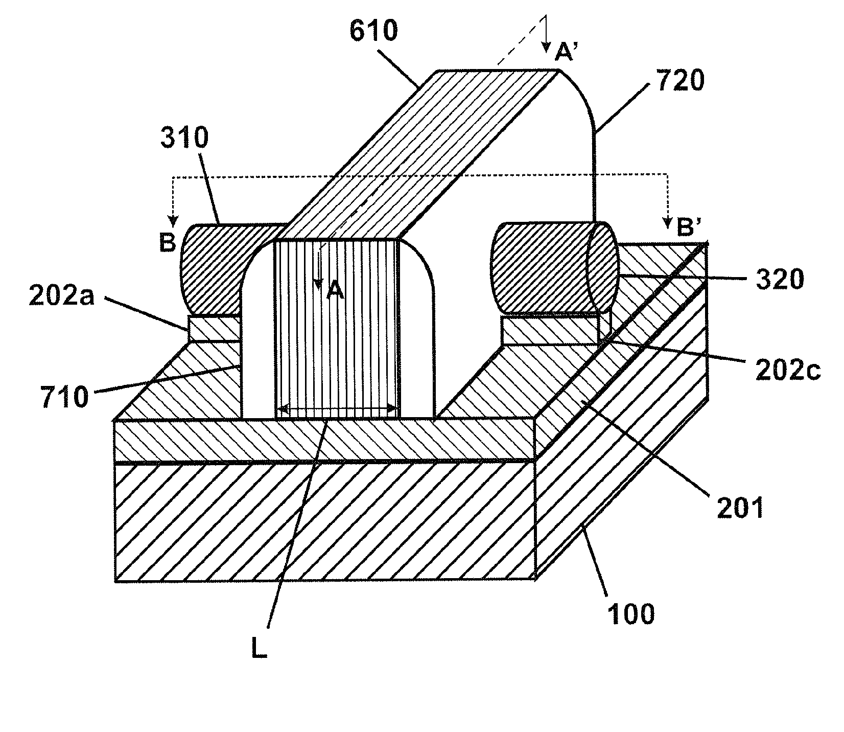
[0037]The present invention is directed to integrated circuits and their processing for the manufacture of semiconductor devices. More particularly, the invention provides a semiconductor device having a transistor and a method for fabrication thereof. Merely by way of example, the invention has been applied to a field effect transistor (FET) device having a gate-all-around cylindrical (GAAC) nanowire. As an example, the FET is based on a silicon-on-insulator (SOI) wafer substrate and method for the manufacture thereof. But it would be recognized that the invention has a much broader range of applicability.

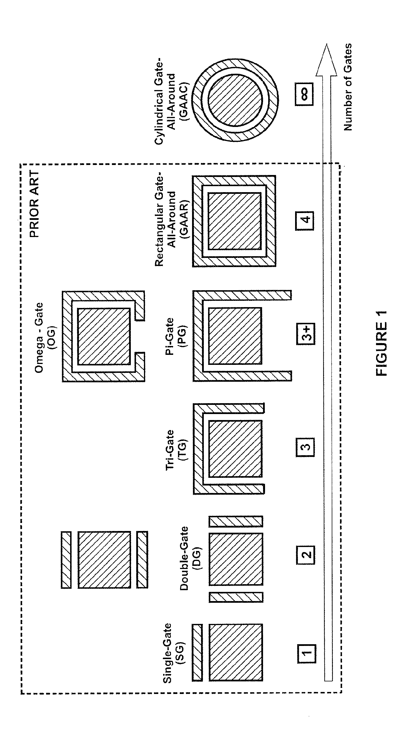
[0038]As discuss above, various conventional techniques have been developed for FET devices. For example, to fabricate devices beyond current scaling limits, alternative gate stack materials, band engineering methods, and alternative transistor structures are all explored rigorously. It has been studied that for FET the single gate full-depleted single-gate SG-FD device cannot be ...


PUM


Abstract

A system and method for integrated circuits with surrounding gate structures are disclosed. The integrated circuits system includes a transistor having a gate all around cylindrical (GAAC) nanowire channel with an interposed dielectric layer. The cylindrical nanowire channel being in a middle section of a semiconductor wire pattern connects the source and drain region positioned at the two opposite end sections of the same wire pattern. A method is provided for manufacturing the integrate circuits system with a GAAC transistor including forming an SOI layer wire pattern on the buried oxide layer of an SOI wafer; forming a cavity underneath the middle section of the wire pattern and shaping the middle section to cylindrically shaped channel; forming a gate electrode surrounding the cylindrical channel region with an interposed gate dielectric layer, the gate electrode being positioned on the buried oxide layer vertically towards the wire pattern; forming the source / drain regions at the two opposite end sections of the wire pattern on either sides of the gate electrode and channel.

Description

CROSS-REFERENCES TO RELATED APPLICATIONS[0001]This application claims priority to Chinese Patent Application No. 200910057965.3, filed Sep. 28, 2009, by inventors De Yuan Xiao et al., commonly assigned and incorporated by reference herein for all purposes.BACKGROUND OF THE INVENTION[0002]The present invention is directed to integrated circuits and their processing for the manufacture of semiconductor devices. More particularly, the invention provides a semiconductor device having a transistor and a method for fabrication thereof. Merely by way of example, the invention has been applied to a field effect transistor (FET) device having a gate-all-around cylindrical (GAAC) nanowire. As an example, the FET is based on a silicon-on-insulator (SOI) wafer substrate and method for the manufacture thereof. But it would be recognized that the invention has a much broader range of applicability.[0003]Integrated circuits or “ICs” have evolved from a handful of interconnected devices fabricated ...

Claims


Application Information

Patent Timeline
Patent Type & Authority Patents(United States)
IPC IPC(8): H01L29/423H01L29/786B82Y10/00H01L29/78H01L29/06H01L29/66
CPCH01L29/42392H01L29/0673H01L29/66795H01L29/0665B82Y10/00H01L29/7854H01L29/78696H01L21/28035H01L29/4916H01L29/42376H01L29/4238H01L21/31133H01L21/324H01L29/6656H01L21/84
Inventor XIAO, DE YUANCHEN, GUO QINGLEE, ROGERYEN, CHIN FUXING, SUHUANG, XIAO LUYANG, YONG SHENG
Owner SEMICON MFG INT (SHANGHAI) CORP
Why Eureka
Try Eureka