Crystal manufacturing apparatus, semiconductor device manufactured using the same, and method of manufacturing semiconductor device using the same

a manufacturing apparatus and semiconductor technology, applied in the direction of crystal growth process, sustainable manufacturing/processing, final product manufacturing, etc., can solve the problem of difficult to manufacture crystals in the desired position on the substrate, and achieve the effect of reducing the number of steps

Inactive Publication Date: 2014-12-02
HIROSHIMA UNIVERSITY
View PDF24 Cites 1 Cited by
  • Summary
  • Abstract
  • Description
  • Claims
  • Application Information

AI Technical Summary

Benefits of technology

[0013]Therefore, the present invention is directed to a solution to the above-described problems, and it is an object of the present invention to provide a crystal manufacturing apparatus capable of manufacturing a crystal in a desired position on a substrate.
[0042]Therefore, according to the present invention, a semiconductor device can be manufactured by a reduced number of steps.

Problems solved by technology

In the conventional method of manufacturing a crystal material, however, a droplet is allowed to fall freely from an initial speed of zero, which makes it difficult to manufacture a crystal in a desired position on a substrate.

Method used


Image

  • Crystal manufacturing apparatus, semiconductor device manufactured using the same, and method of manufacturing semiconductor device using the same
  • Crystal manufacturing apparatus, semiconductor device manufactured using the same, and method of manufacturing semiconductor device using the same
  • Crystal manufacturing apparatus, semiconductor device manufactured using the same, and method of manufacturing semiconductor device using the same

Examples


Embodiment Construction

[0084]An embodiment of the present invention will be described in conjunction with the accompanying drawings in which the same or corresponding portions are designated by the same reference characters and their description will not be repeated.

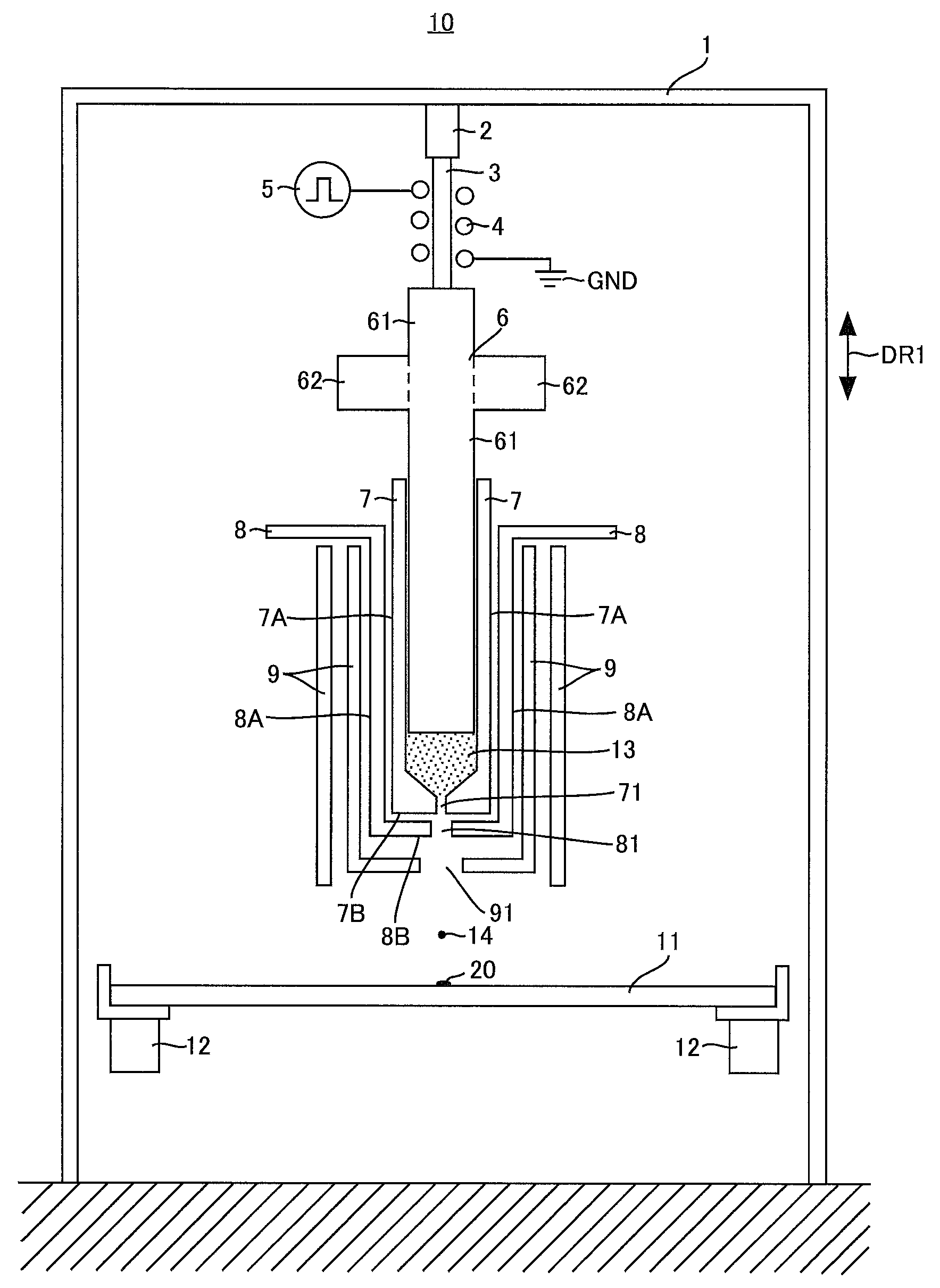
[0085]FIG. 1 is a schematic view of a crystal manufacturing apparatus according to an embodiment of the present invention. Referring to FIG. 1, the crystal manufacturing apparatus 10 according to the embodiment includes a mount 1, a spring 2, a magnetic body 3, a coil 4, a power supply circuit 5, a piston 6, a cylinder 7, a heater 8, reflector 9, a substrate 11, and an XY stage 12.

[0086]The spring 2 has one end fixed to the mount 1 and the other end connected to one end of the magnetic body 3.

[0087]The magnetic body 3 has one end connected to the spring 2 and the other end coupled to one end of the piston 6. The coil 4 is wound around the magnetic body 3 and electrically connected between the power supply circuit 5 and a ground node GND.

[0088]...


PUM

PropertyMeasurementUnit
diameteraaaaaaaaaa
diameteraaaaaaaaaa
lengthaaaaaaaaaa

Abstract

A crystal manufacturing apparatus capable of manufacturing a crystal in a desired position on a substrate is provided. A spring has one end fixed to a mount and the other end coupled to a magnetic body. The magnetic body has one end coupled to the spring and the other end coupled to a piston. A coil is wound around the magnetic body and electrically connected between a power supply circuit and a ground node (GND). The piston has a linear member inserted in a cylinder. The cylinder has a hollow columnar shape and a small hole at a bottom surface. The cylinder holds a silicon melt. A substrate is supported by an XY stage to be opposed to the small hole of the cylinder. The power supply circuit passes pulse shaped current through the coil to move the piston in an up-down direction (DR1). As a result, a droplet is discharged toward the substrate from the small hole at an initial speed of 1.02 m / s.

Description

RELATED APPLICATIONS[0001]The present application is national phase of PCT / JP2009 / 004209 filed Aug. 28, 2009, and claims priority from Japanese Application Number 2008-223419 filed Sep. 1, 2008 and Japanese Application Number 2009-049616 filed Mar. 3, 2009.TECHNICAL FIELD[0002]The present invention relates to a crystal manufacturing apparatus, a semiconductor device manufactured using the same, and a method of manufacturing a semiconductor device using the same. The invention relates more specifically to a crystal manufacturing apparatus that manufactures crystalline semiconductor using a melt of a constituent element of the semiconductor, a semiconductor device manufactured using the same, and a method of manufacturing a semiconductor device using the same.BACKGROUND ART[0003]There is a known method of manufacturing a crystal material by allowing a part of a melt of a metal containing material to fall freely (which refers to a fall from an initial speed of zero) through a small hol...

Claims


Application Information

Patent Timeline
Patent Type & Authority Patents(United States)
IPC IPC(8): H01L21/336C30B29/06C30B35/00H01L29/786H01L31/18H01L27/12C01B33/02C30B28/06H01L21/67H01L21/02
CPCH01L21/02422C30B29/06H01L27/1218C01B33/02H01L27/1292C30B28/06H01L27/1285H01L31/1804H01L31/1892H01L29/78636H01L21/02667H01L21/67248Y02E10/547H01L21/02625H01L21/6715C30B35/00H01L21/02532H01L29/78603H01L27/1214Y02P70/50
Inventor HIGASHI, SEIICHIROKOBA, NAOHIRO
Owner HIROSHIMA UNIVERSITY
Why Eureka
Try Eureka