Electronic devices, circuits and their manufacture

a technology of electronic circuits and electronic devices, applied in the direction of microstructural devices, microstructured devices, organic semiconductor devices, etc., can solve the problems of increasing the total manufacturing time, undesirable removal of semiconductive materials, and undetectable distortion of the upper layer of semiconductive materials by the printing technique, so as to reduce the smearing or transfer of materials, improve the cleanness of aperture edges, and reduce the effect of smearing

Active Publication Date: 2015-09-01
PRAGMATIC PRINTING
View PDF15 Cites 0 Cited by
  • Summary
  • Abstract
  • Description
  • Claims
  • Application Information

AI Technical Summary

Benefits of technology

[0007]Certain embodiments of the invention aim to provide methods which facilitate the manufacture of electronic devices and / or circuits comprising a plurality of devices. Certain embodiments aim to provide methods of manufacture which are faster than certain prior art techniques. Further embodiments aim to provide methods of manufacture which are compatible with fast, high volume production of electronic devices and / or circuits. Certain embodiments aim to provide methods of manufacturing electronic circuits comprising a plurality of electronic devices formed on a common, flexible substrate. Certain embodiments aim to provide methods of manufacturing electronic devices and / or circuits having a reduced number of steps compared with prior art techniques.
[0179]Certain methods embodying the invention are applicable to device templates which are intended for an electronic or photonic device. The apertures formed in the active layer of the device template by the method may typically be small apertures, having dimensions in the range 20 to 1000 nm, or 100 to 300 nm. However, methods embodying the invention may also be used to form larger apertures (having dimensions of 10 micrometres or more). This may be particularly advantageous compared to direct beam lithography to form large apertures in devices or device templates, as each part of an isolating area will need to be written by the beam used, leading to long processing times.

Problems solved by technology

Clearly, whilst this imprinting or embossing technique offers some advantages in terms of facilitating the initial patterning of the upper layer, it has disadvantages as a technique for forming insulative features, because additional processing steps are required.
Furthermore, this imprinting technique may undesirably distort the upper layer of semiconductive material, at least in the vicinity of each embossed trench.
Furthermore, the etching technique required to expose the underlying substrate may result in undesirable removal of semiconductive material from other portions of the semiconductive layer.
It will be appreciated that in the fabrication of electronic devices and circuits, disadvantages associated with additional processing steps include the fact that the total manufacturing time is increased, and so are the complexity and costs of the overall process.
An additional problem with existing techniques for etching features in semiconductive materials is that those techniques may be suitable for use with certain materials but not others.

Method used


Image

  • Electronic devices, circuits and their manufacture
  • Electronic devices, circuits and their manufacture
  • Electronic devices, circuits and their manufacture

Examples


Embodiment Construction

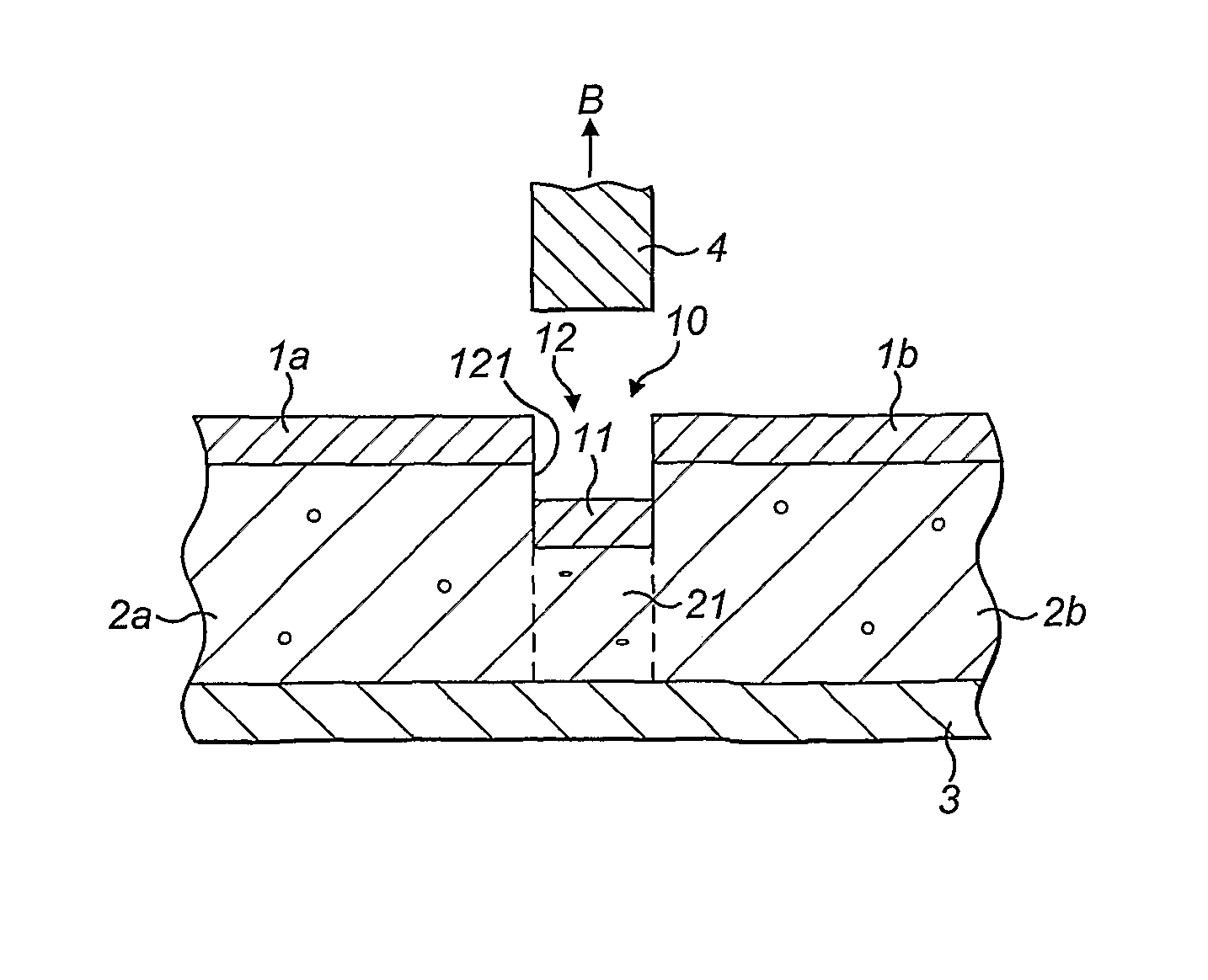
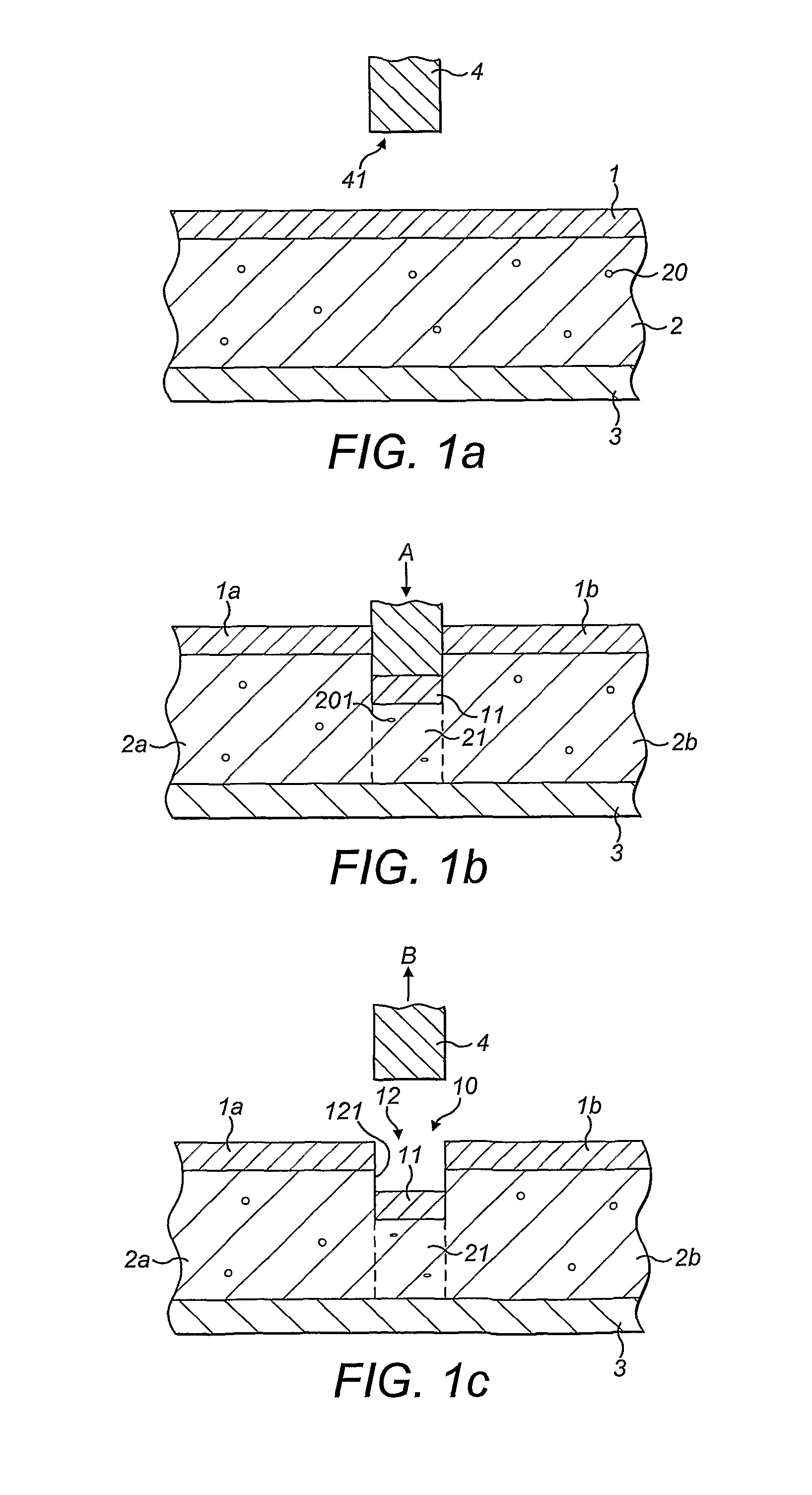
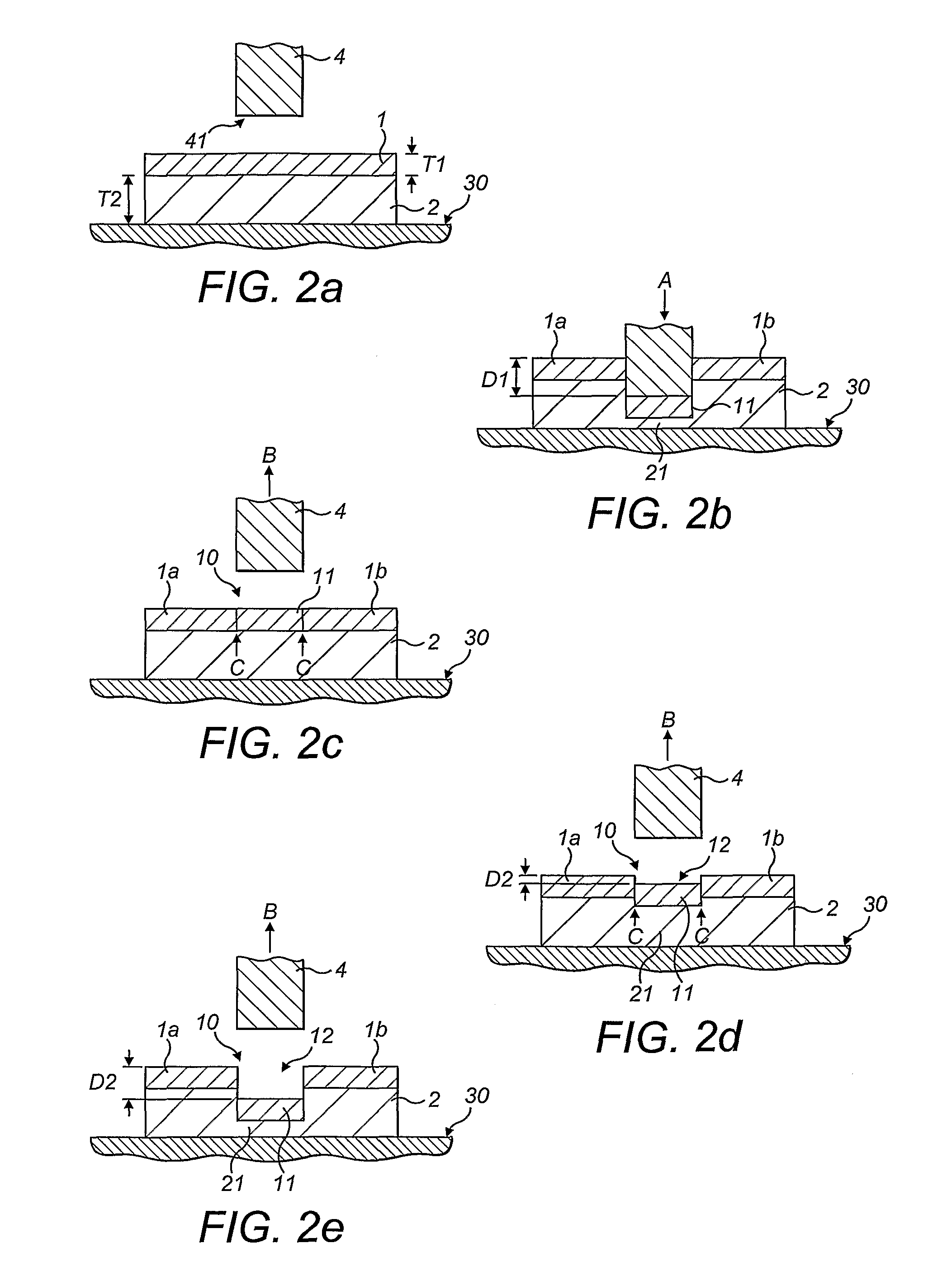
[0219]Referring now to FIGS. 1a-1c, in a first method embodying the invention a layer of semiconductive material 1 is provided, supported by a layer 2 of insulative and compressible material.

[0220]The insulative layer 2 is itself supported by an underlying substrate layer 3, in this example formed of substantially non-compressible material. The semiconductive layer 1, compressible layer 2, and substrate or backing layer 3 can together be described as forming a multi-layer device substrate. It will be appreciated that a wide variety of techniques known in the art may be used to fabricate such a multi-layer structure, and embodiments of the invention may utilise any suitable such techniques, for example techniques selected to suit the particular material or materials of each layer. In certain embodiments, for example, the semiconductive layer 1 is a layer of organic semiconductive material, which may be formed over the compressible layer by spin-coating. In this first example, the mat...


PUM

PropertyMeasurementUnit
widthaaaaaaaaaa
widthaaaaaaaaaa
widthaaaaaaaaaa

Abstract

A method of manufacturing an electronic device, comprising a layer of semiconductive material and at least one insulative feature arranged to interrupt the layer of semiconductive material, comprises: providing a layer of semiconductive material, and a layer of compressible material supporting the layer of semiconductive material; and forming the or each insulative feature by a method comprising displacing a respective selected portion of the layer of semiconductive material towards the compressible material so as to compress compressible material under the or each displaced portion and separate at least partly the or each displaced portion from undisplaced semiconductive material.

Description

CROSS REFERENCE TO RELATED APPLICATIONS[0001]This is the U.S. National Stage of International Application No. PCT / GB2010 / 050123, filed Jan. 27, 2010, which in turn claims the benefit of Great Britain Application No. GB0901389.7, filed Jan. 28, 2009.FIELD OF THE INVENTION[0002]The present invention relates to electronic devices and electronic circuits and methods of manufacturing such devices and circuits. In particular, although not exclusively, certain embodiments of the invention are concerned with nano electronic devices and circuits and their manufacture, that is devices and circuits having features with dimensions in the range of 10 to 300 nanometres.BACKGROUND TO THE INVENTION[0003]Electronic devices and features comprising a layer of semiconductive material patterned with insulated features are known. Examples of such devices and circuits are disclosed in WO 02 / 086973 A2, WO 2006 / 008467 A1, and WO 2006 / 120414 A2. The contents of each of these documents are incorporated herein...

Claims


Application Information

Patent Timeline
Patent Type & Authority Patents(United States)
IPC IPC(8): H01L51/00H01L21/764H01L27/28H01L51/05
CPCH01L51/0014H01L21/764H01L27/28H01L51/0023H01L51/0036H01L51/0575H01L2251/105H10K71/20H10K71/621H10K85/113H10K10/20H10K71/821H10K19/80B81C1/00095B81C1/00214B81C1/0046H01L21/70H01L21/76H01L21/768H01L21/77H01L31/18H01L33/005H10K19/00
Inventor SONG, AIMINWHITELEGG, STEPHENSUN, YANMINGLIN, SHIWEI
Owner PRAGMATIC PRINTING
Why Eureka
Try Eureka