Single-band and dual-band infrared detectors

a single-band, infrared detector technology, applied in the field of single-band infrared detectors, can solve the problems of image blurring, pbp structure has its own problems, and holes have more difficulty in diffusing along the perpendicular direction toward the collecting contact than diffusing laterally,

Active Publication Date: 2015-01-06
CALIFORNIA INST OF TECH
View PDF25 Cites 7 Cited by
  • Summary
  • Abstract
  • Description
  • Claims
  • Application Information

AI Technical Summary

Problems solved by technology

The fact that holes have more difficulty diffusing along the perpendicular direction toward the collecting contact than diffusing laterally can be very problematic in a focal plane array (FPA).
In a planar-processed FPA with non-reticulated pixels, strong lateral diffusion means that minority carriers can spread easily to neighboring pixels, resulting in image blurring.
However, the pBp structure has its own problems.
.), the pBp design is susceptible to this mechanism.
This can result in a sizable dark current that reduces detector sensitivity.

Method used


Image

  • Single-band and dual-band infrared detectors
  • Single-band and dual-band infrared detectors
  • Single-band and dual-band infrared detectors

Examples


Embodiment Construction

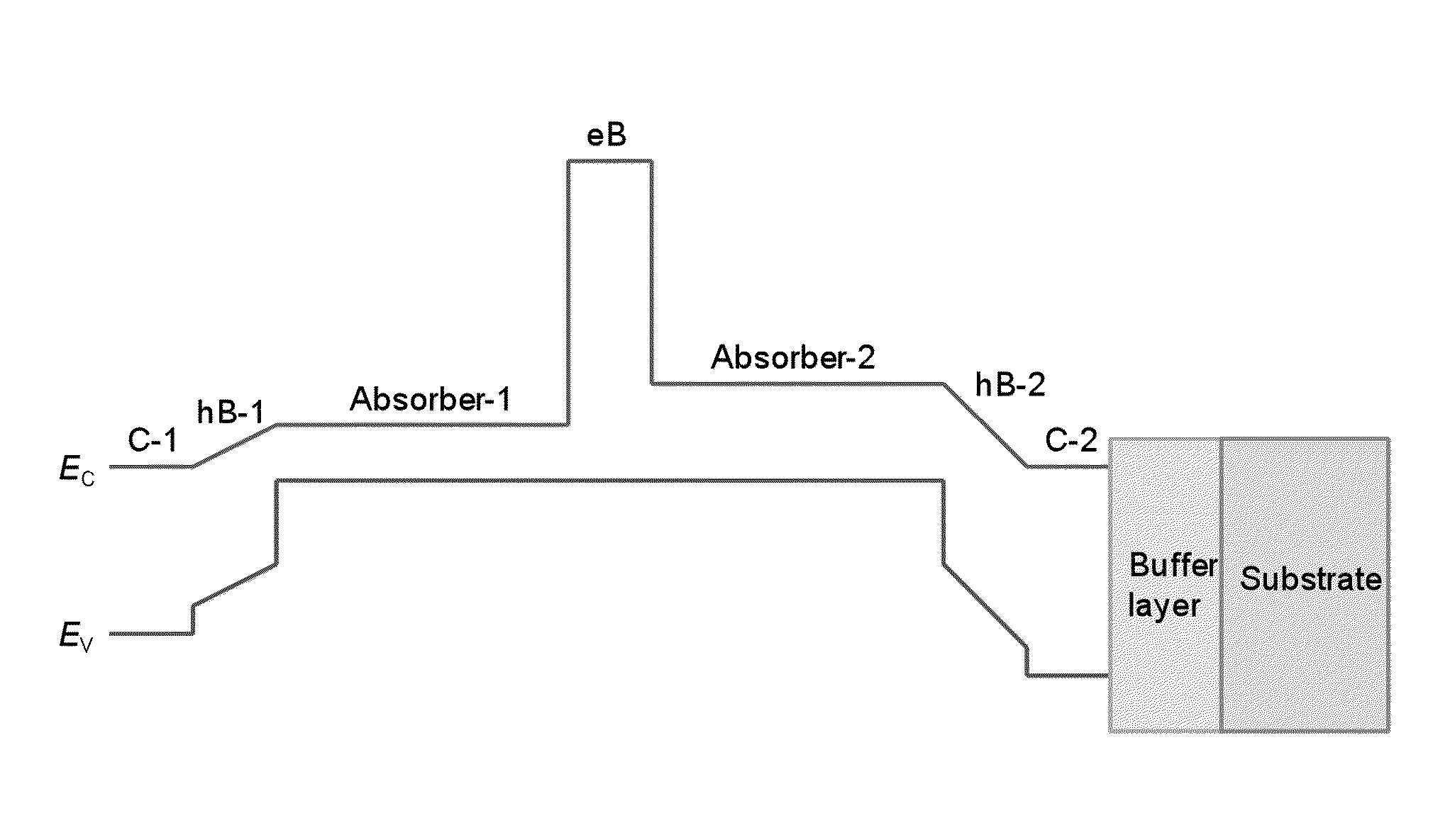
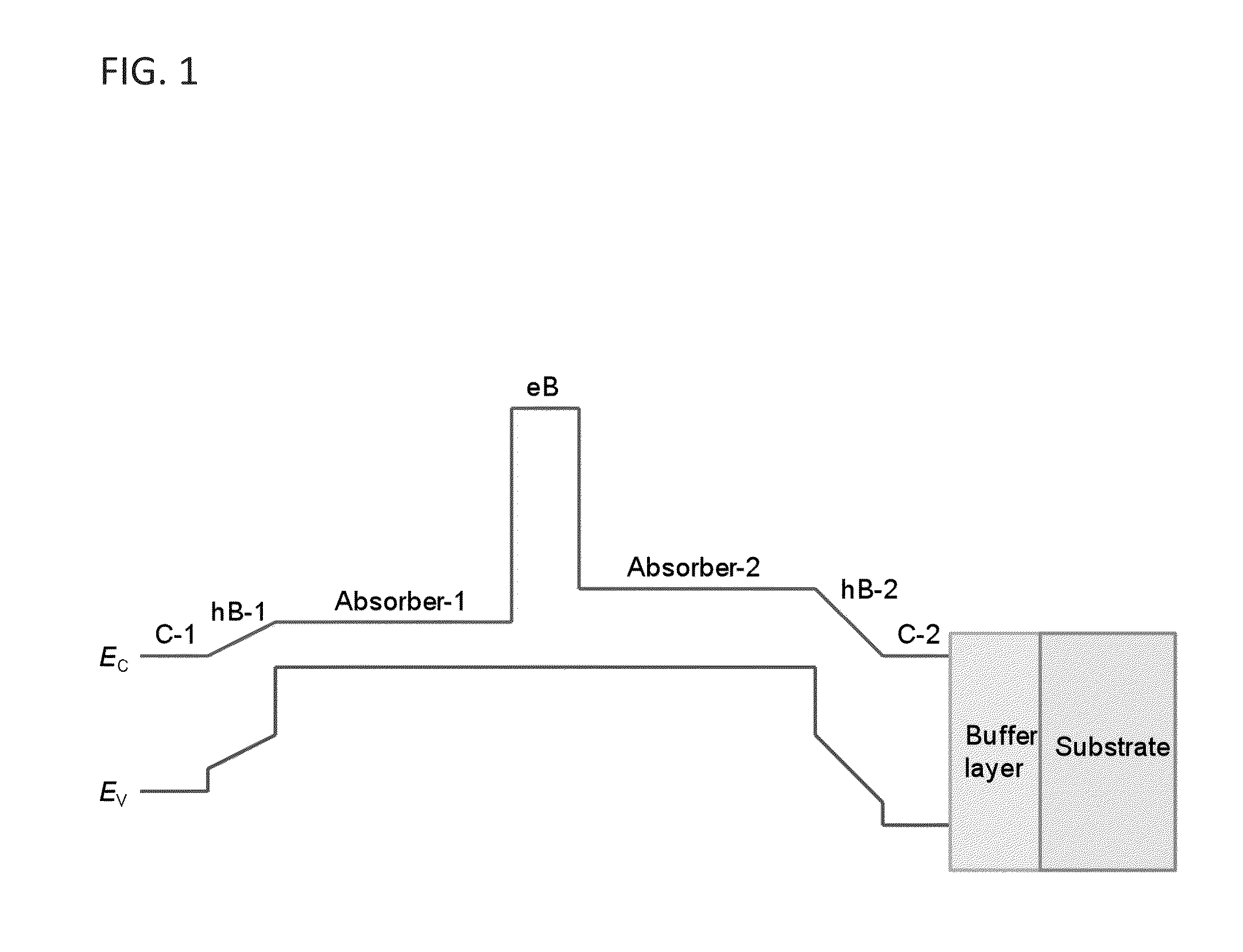
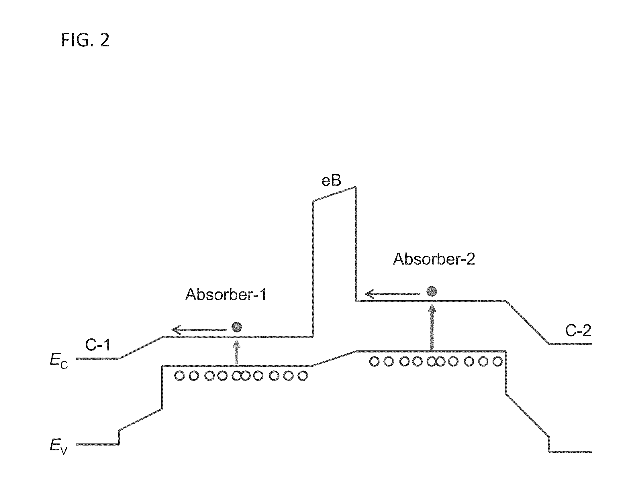
[0058]Bias-switchable dual-band infrared are described in the embodiments set forth herein. As will be described embodiments of the infrared detectors are based on a back-to-back heterojunction diode design. In these embodiments, the detector consists generally of a sequential structure that includes:[0059]a top contact layer,[0060]a unipolar hole barrier layer,[0061]an absorber layer,[0062]a unipolar electron barrier,[0063]a second absorber,[0064]a second unipolar hole barrier, and[0065]a bottom contact layer.

[0066]In addition, as will be discussed in greater detail below, by substantially reducing the width of one of the absorber layers, a single-band infrared detector can also be formed.

Definitions

[0067]An absorber layer or structure, as used herein is a layer of a semiconducting material or materials having a bandgap structure where photons impinging on the material with sufficient energy excite electrons across the material's bandgap to produce photocurrents.

[0068]A unipolar ba...


PUM


Abstract

Bias-switchable dual-band infrared detectors and methods of manufacturing such detectors are provided. The infrared detectors are based on a back-to-back heterojunction diode design, where the detector structure consists of, sequentially, a top contact layer, a unipolar hole barrier layer, an absorber layer, a unipolar electron barrier, a second absorber, a second unipolar hole barrier, and a bottom contact layer. In addition, by substantially reducing the width of one of the absorber layers, a single-band infrared detector can also be formed.

Description

CROSS-REFERENCE TO RELATED APPLICATIONS[0001]The current application claims priority to U.S. Provisional Application No. 61 / 569,375, filed Dec. 12, 2011, the disclosure of which is incorporated herein by reference.STATEMENT OF FEDERAL FUNDING[0002]The invention described herein was made in the performance of work under a NASA contract, and is subject to the Provisions of Public Law 96-517 (35 USC 202) in which the Contractor has elected to retain title.FIELD OF THE INVENTION[0003]The current invention is directed to an infrared detector; and more particularly to a bias-switchable dual-band or single-band infrared detector.BACKGROUND OF THE INVENTION[0004]HgCdTe-based bias-switchable dual-band (two-color) infrared detectors have been reported in the literature since the early 1990s. The typical device structure consists of two back-to-back infrared photodiodes, each designed to detect a particular color band. The two diodes are monolithically integrated, typically in an n-P-N (capita...

Claims


Application Information

Patent Timeline
Patent Type & Authority Patents(United States)
IPC IPC(8): H01L29/74H01L31/02H01L31/109
CPCH01L31/02016H01L31/109H01L31/101H01L31/1013H01L31/02019
Inventor TING, DAVID Z.GUNAPALA, SARATH D.SOIBEL, ALEXANDERNGUYEN, JEANKHOSHAKHLAGH, AREZOU
Owner CALIFORNIA INST OF TECH
Why Eureka
Try Eureka