Component aligning apparatus and electronic component manufacturing method

a technology of electronic components and aligning apparatus, which is applied in the manufacture of capacitors, programmed manipulators, ammunition loading, etc., can solve the problems of not being able to adapt to the thickness reduction of chip-type electronic components, and achieve the effect of high precision and eas

Active Publication Date: 2015-01-27
MURATA MFG CO LTD
View PDF10 Cites 2 Cited by
  • Summary
  • Abstract
  • Description
  • Claims
  • Application Information

AI Technical Summary

Benefits of technology

[0012]Preferred embodiments of the present invention provide a component aligning apparatus which enables a plurality of chip-type electronic components to be aligned in proper orientation even if the chip-type electronic components are made thinner, and accordingly makes it possible to apply, for example, conductive paste to the chip-type electronic components with high precision. Also, preferred embodiments of the present invention provide an electronic component manufacturing method using the component aligning apparatus.
[0015]In another specific preferred embodiment of the component aligning apparatus according to the present invention, the component aligning apparatus further includes a feed-in jig to feed a single one of the electronic components into each of the through-holes of the guide plate, the feed-in jig being mounted on top of a stacked body in which the guide plate and the component aligning jig are stacked, the feed-in jig includes a plurality of recesses on one surface, and the recesses are arranged so as to accommodate each of the electronic components with the WL surface of each of the electronic components facing down. Accordingly, by placing the feed-in jig on top of the stacked body in which the guide plate and the component aligning jig are stacked so that the recesses of the feed-in jig face the through-holes of the guide plate, the electronic components accommodated in the recesses of the feed-in jig can be easily dropped into the through-holes and, therefore, the electronic components can be accommodated in the accommodating recesses of the component aligning jig in proper orientation more reliably.
[0017]In yet still another specific preferred embodiment of the component aligning apparatus according to the present invention, the first and second stripe-shaped spaces define a cross-shaped space in plan view. In this case, since the first and second stripe-shaped spaces are substantially orthogonal to each other, chip-type electronic components supplied in various orientations can each be accommodated in the first or second stripe-shaped space reliably and easily.
[0019]In a specific preferred embodiment of the electronic component manufacturing method according to the present invention, the electronic component manufacturing method further includes the steps of abutting an adhesive holding member onto the WT surface on the upper side of the electronic components accommodated in the accommodating recesses of the aligning jig, transporting the electronic components while holding the electronic components by the adhesive holding member, by moving the adhesive holding member away from the aligning jig, and immersing the electronic components into a conductive paste from the WT surface on a side of the electronic components opposite to a side stuck on the adhesive holding member. In this case, after aligning the electronic components by the component aligning apparatus according to a preferred embodiment of the present invention, by transporting the electronic components on the adhesive holding member, and bringing the electronic components held by the adhesive holding member into contact with the conductive paste in proper orientation, the conductive paste can be applied to the electronic components with high precision from the WT surface side of the electronic components.
[0022]In the component aligning apparatus according to various preferred embodiments of the present invention, since the shortest separation S between the inside surfaces of each accommodating recess of the component aligning jig is set as W>S>T, the electronic components can be reliably positioned in the accommodating recesses in proper orientation, even as the electronic components are made thinner. Accordingly, by simply inserting the electronic components into the accommodating recesses of the component aligning apparatus mentioned above in accordance with the electronic component manufacturing method according to another preferred embodiment of the present invention, a plurality of electronic components can be aligned and held in a plurality of accommodating recesses reliably and properly.
[0023]Thus, for example, it becomes possible to pick up the plurality of aligned electronic components by using the adhesive holding member or the like, and perform application of conductive paste or the like with high precision and ease.

Problems solved by technology

Accordingly, in the case where the aligning apparatus 1001 having the though-holes 1003a that are circular in plan view as described in Japanese Unexamined Patent Application Publication No. 2001-345240 is used, it is not possible to adapt to thickness reduction of chip-type electronic components.

Method used


Image

  • Component aligning apparatus and electronic component manufacturing method
  • Component aligning apparatus and electronic component manufacturing method
  • Component aligning apparatus and electronic component manufacturing method

Examples


Embodiment Construction

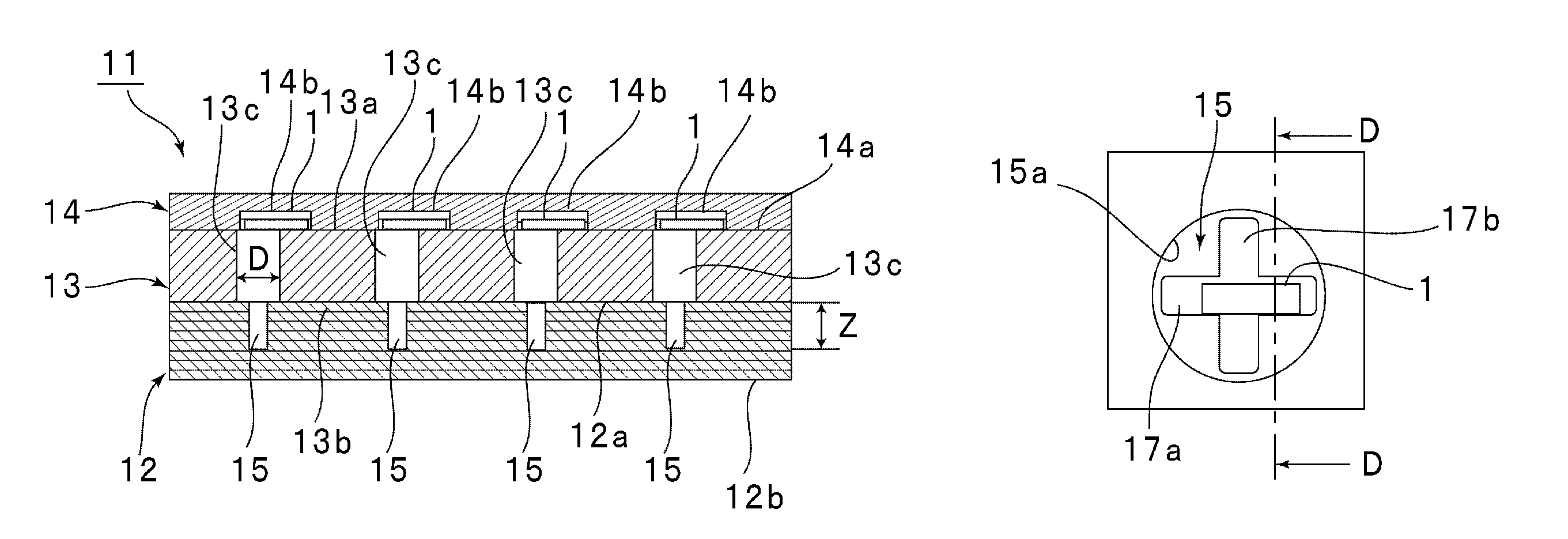
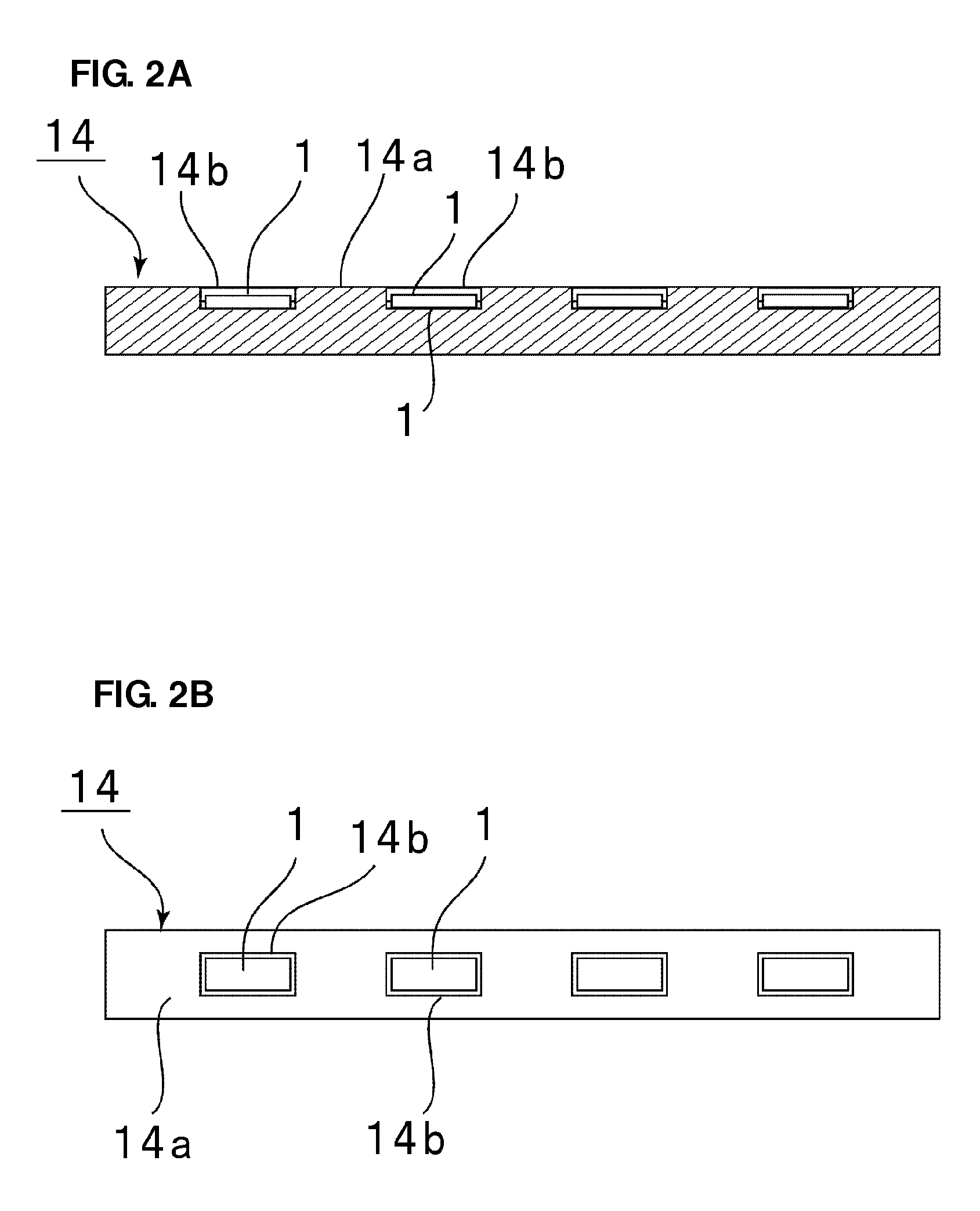
[0044]The present invention will be explained below by describing specific preferred embodiments of the present invention with reference to the drawings.

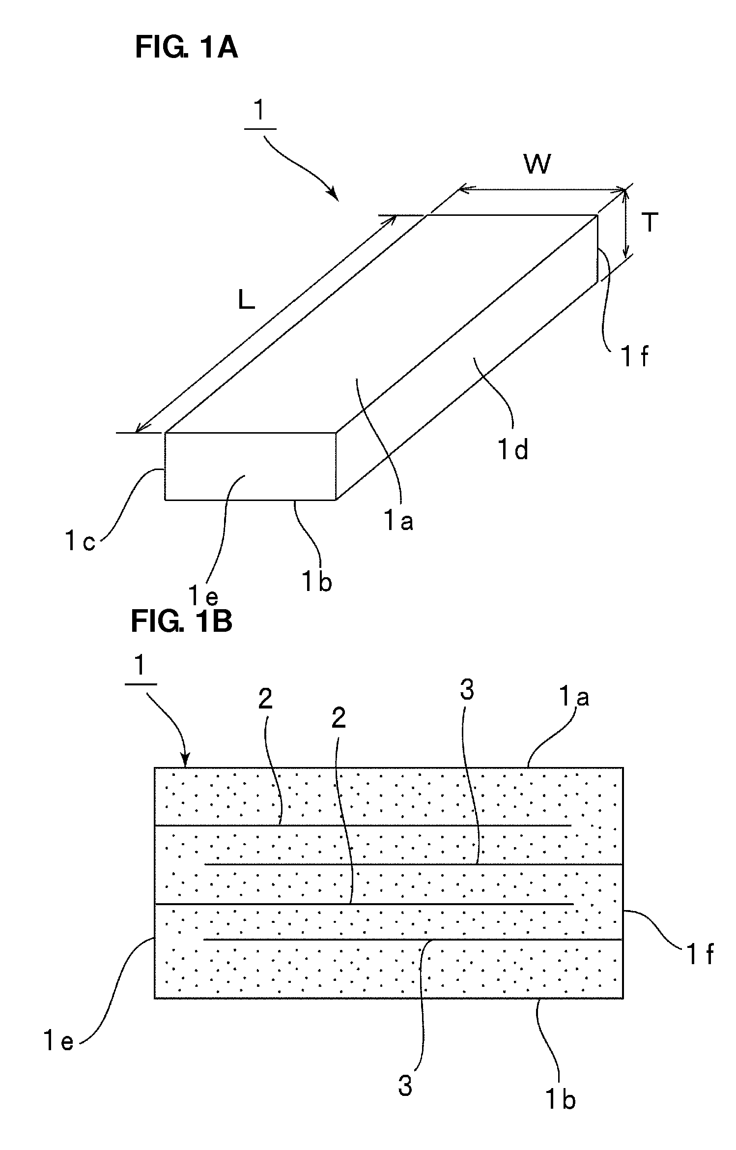
[0045]FIG. 1A is a perspective view and FIG. 1B is a front sectional view showing each electronic component to be aligned according to a preferred embodiment of the present invention.

[0046]Chip-like electronic components 1 each preferably have a rectangular parallelepiped shape. Let L, W, and T be the length, width, and thickness dimensions of the electronic components 1, respectively. Depending on the case, for ease of explanation, the outer surfaces of the electronic components 1 will be expressed by referring the surface along the length direction and the width direction as WL surface, the surface along the width direction and the thickness direction as WT surface, and the surface along the length direction and the thickness direction as LT surface. For example, an upper surface 1a and a lower surface 1b of the electronic compone...


PUM

PropertyMeasurementUnit
lengthaaaaaaaaaa
widthaaaaaaaaaa
thicknessaaaaaaaaaa

Abstract

A component aligning apparatus includes a component aligning jig, in which electronic components to be aligned have a rectangular parallelepiped shape whose length dimension is L, width dimension is W, and thickness dimension is T, the component aligning jig includes electronic component accommodating recesses opening on a surface, the depth Z of the accommodating recesses is shorter than the length L of the electronic components so that a single electronic component is held in each of the electronic component accommodating recesses while partially projecting upwards from each of the recesses with the WT surface on one side facing up, and letting s be the shortest separation that is larger than the thickness T and is the narrowest distance between opposing inside surfaces of each of the accommodating recesses when each of the accommodating recesses is seen in plan view, W>S>T.

Description

BACKGROUND OF THE INVENTION[0001]1. Field of the Invention[0002]The present invention relates to an apparatus for aligning electronic components such as ceramic electronic components, and an electronic component manufacturing method using the apparatus, for example, and relates to a component aligning apparatus for aligning electronic components when forming external electrodes, and an electronic component manufacturing method using the apparatus, for example.[0003]2. Description of the Related Art[0004]In the related art, in chip-type electronic components, external electrodes are formed by applying conductive paste to the outer surface of the chip-type electronic components. To apply such conductive paste to chip-type electronic components with high precision, an aligning apparatus 1001 shown in FIG. 15 is used in Japanese Unexamined Patent Application Publication No. 2001-345240.[0005]In the aligning apparatus 1001, a guide plate 1003 having a plurality of through-holes 1003a is ...

Claims


Application Information

Patent Timeline
Patent Type & Authority Patents(United States)
IPC IPC(8): B23P19/00H01G4/005H01G4/30H01G13/00
CPCH01G4/005H01G4/30H01G13/00H01G13/006H01G4/232Y10T29/49002Y10T29/4913Y10T29/53257Y10T29/53261Y10T29/53265H01G4/12
Inventor MIYAZAKI, TOSHIKI
Owner MURATA MFG CO LTD
Why Eureka
Try Eureka