Semiconductor device having insulating layer formed through oxidization of electrode

a technology of oxidizing electrodes and semiconductors, applied in the manufacture of flux-sensitive heads, instruments, and record information storage, etc., can solve the problems of reducing the etching damage affecting the etching speed of the tunnel insulating layer, and affecting the etching speed of the upper electrode pattern

Active Publication Date: 2015-01-27
SK HYNIX INC
View PDF1 Cites 8 Cited by
  • Summary
  • Abstract
  • Description
  • Claims
  • Application Information

AI Technical Summary

Benefits of technology

[0009]An embodiment of the present invention is directed to a method for fabricating a semiconductor device, which can prevent an etching defect caused in a process of fabricating a magnetic tunnel junction pattern.
[0012]In a method for fabricating a semiconductor device having a magnetic tunnel junction in accordance with the present invention, since a lower electrode layer is not separated through etching but through oxidation, an etching failure due to loss of an etching margin is prevented. Further, since a second lower electrode layer is not etched, etching damage of an upper electrode pattern is reduced.

Problems solved by technology

Therefore, the DRAM has a large power loss.
On the other hand, a flash memory, while having characteristics of non-volatility and high integration, has a slow operating speed.
For example, in a process of patterning and subsequently cleaning a magnetoresistive element, a tunnel insulating layer interposed between two ferromagnetic layers may be lost or the ferromagnetic layer may be exposed to the outside.

Method used


Image

  • Semiconductor device having insulating layer formed through oxidization of electrode
  • Semiconductor device having insulating layer formed through oxidization of electrode
  • Semiconductor device having insulating layer formed through oxidization of electrode

Examples


Embodiment Construction

[0015]Exemplary embodiments of the present invention will be described below in more detail with reference to the accompanying drawings. The present invention may, however, be embodied in different forms and should not be construed as limited to the embodiments set forth herein. Rather, these embodiments are provided so that this disclosure will be thorough and complete, and will fully convey the scope of the present invention to those skilled in the art. Throughout the disclosure, like reference numerals refer to like parts throughout the various figures and embodiments of the present invention.

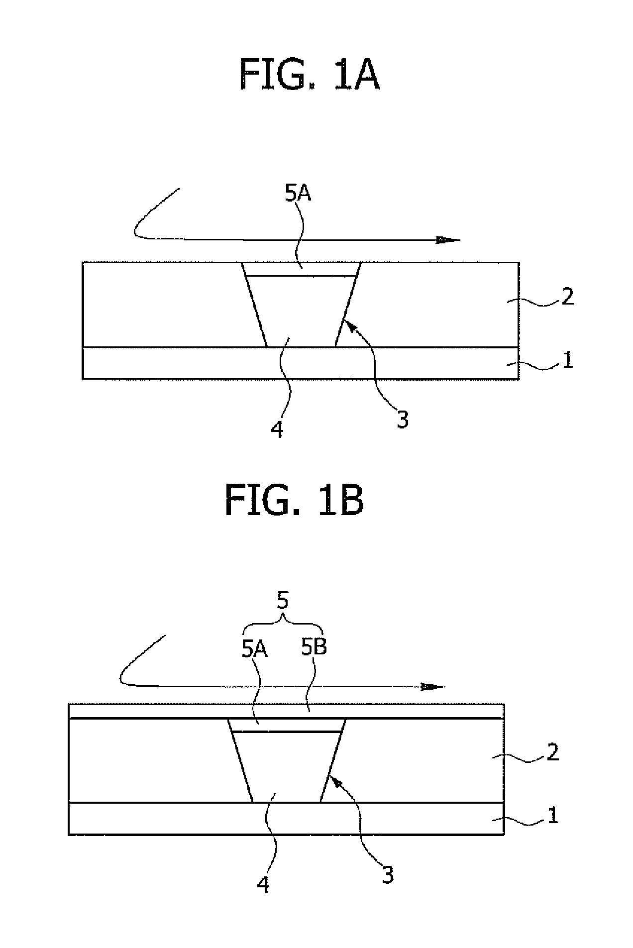
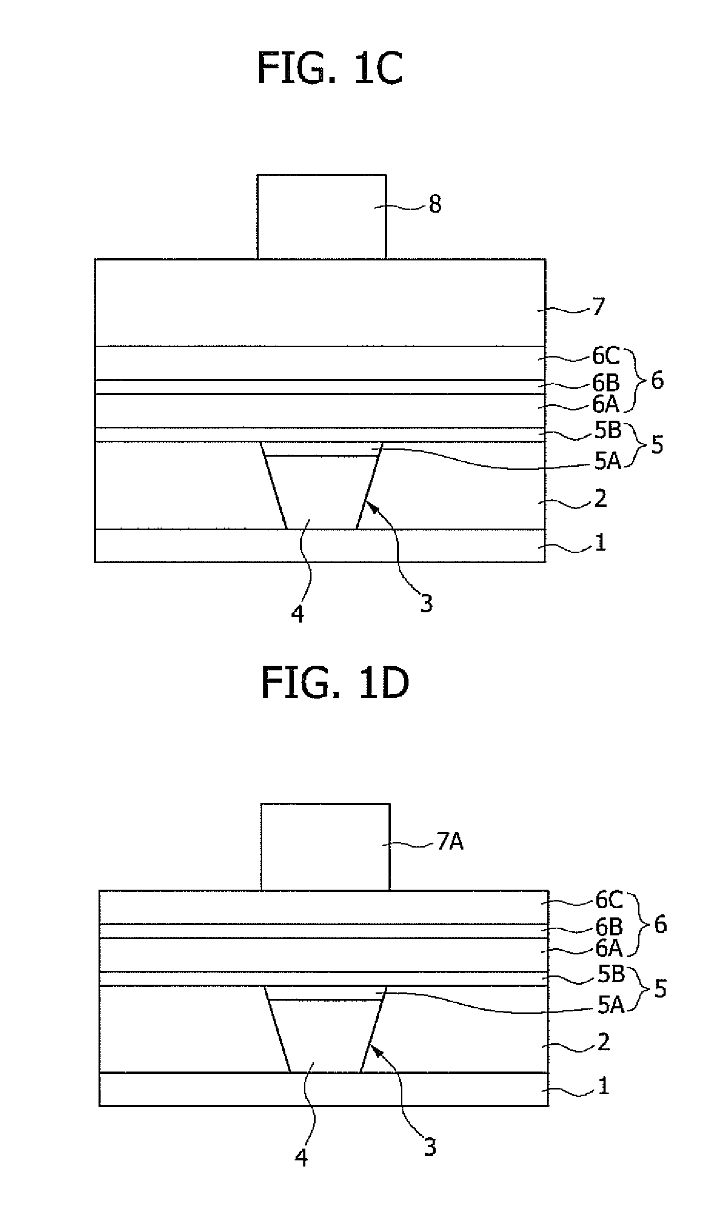
[0016]FIGS. 1a to 1e are sectional views illustrating a method for fabricating a spin transfer torque RAM (STTRAM).

[0017]As illustrated in FIG. 1a, a first interlayer insulating layer 2 is formed on a substrate having a bottom layer 1 formed thereon.

[0018]A transistor for selecting a magnetic tunnel junction is disposed on the bottom layer 1.

[0019]The first interlayer insulating layer 2 func...


PUM


Abstract

In a method for fabricating a semiconductor device, a conductive layer is formed on a substrate, where the substrate has a bottom layer formed thereon. A magnetic tunnel junction layer is formed on the conductive layer. The magnetic tunnel junction layer is patterned using an etching gas containing oxygen. An insulating layer is formed by oxidizing the conductive layer exposed outside the patterned magnetic tunnel junction layer using the etching gas.

Description

CROSS-REFERENCE TO RELATED APPLICATIONS[0001]The present application claims priority of Korean Patent Application No. 10-2011-0078971, filed on Aug. 9, 2011, which is incorporated herein by reference in its entirety.BACKGROUND[0002]1. Field[0003]Exemplary embodiments of the present invention relate to a method for fabricating a semiconductor device, and more particularly, to a method for fabricating a semiconductor device, which can prevent an etching defect caused in a process of fabricating a magnetic tunnel junction pattern.[0004]2. Description of the Related Art[0005]A dynamic random access memory (DRAM) is a representative semiconductor memory having characteristics of high-speed operation and high integration. On the other hand, the DRAM being a non-volatile memory loses data when power is turned off, and refresh of data is continuously performed during the operation of the DRAM. Therefore, the DRAM has a large power loss. On the other hand, a flash memory, while having charac...

Claims


Application Information

Patent Timeline
Patent Type & Authority Patents(United States)
IPC IPC(8): H01L29/82G11B5/33G11B5/127H01L43/08H01L43/10H01L43/12
CPCH01L43/08H01L43/10H01L43/12G11C11/161H10N50/10H10N50/01H10N50/85G11C11/15
Inventor LEE, MIN SUKJUNG, BO KYOUNG
Owner SK HYNIX INC
Why Eureka
Try Eureka