Method for reducing irregularities at the surface of a layer transferred from a source substrate to a glass-based support substrate

a technology of source substrate and support substrate, which is applied in the direction of basic electric elements, electrical equipment, semiconductor devices, etc., can solve the problems of high cost of such structures, difficult to replace traditional silicon support substrates with glass-based support substrates, and generate particularly numerous and deep surface irregularities at separation zones. , to achieve the effect of reducing the surface area of plateaus, reducing the number and depth, and reducing the number of irregularities

Active Publication Date: 2015-02-03
SOITEC SA
View PDF15 Cites 2 Cited by
  • Summary
  • Abstract
  • Description
  • Claims
  • Application Information

AI Technical Summary

Benefits of technology

[0012]The aim of the present invention is to provide a method for making improved-quality SiOG structures in which the surface of separation between the layer transferred to the glass-based support substrate and the rest of the source substrate presents reduced surface irregularities, in particular, with a decrease of the surface area of plateaus and a decrease of the number and depth of canyons encircling the plateaus.
[0013]Moreover, the present invention also aims at avoiding the need for long CMP polishing, in order to speed up industrial processes, and save raw materials.

Problems solved by technology

Because of its rather high thickness, in particular as compared to the other parts, a major fraction of the cost of such structures has been the cost of the silicon substrate that supports the oxide layer, topped by the thin silicon layer.
However, it is not a simple matter to replace a traditional silicon support substrate with a glass-based support substrate.
Indeed, splitting the source substrate at the separation zone generates particularly numerous and deep surface irregularities, as represented in FIG. 2.
However, such polishing is long and expensive, in particular if the plateaus present a high-density of microroughnesses 42.
An important amount of high-grade silicon is therefore wasted.

Method used


Image

  • Method for reducing irregularities at the surface of a layer transferred from a source substrate to a glass-based support substrate
  • Method for reducing irregularities at the surface of a layer transferred from a source substrate to a glass-based support substrate
  • Method for reducing irregularities at the surface of a layer transferred from a source substrate to a glass-based support substrate

Examples


Embodiment Construction

[0042]Referring to the drawings, a method according to a possible embodiment of the invention will now be described.

[0043]Glass is a material with a limited stiffness, with a Young's modulus of about 74 GPa. Most metals have a higher stiffness, and silicon has, for example, a Young's modulus varying from 130 GPa for [100] crystallographic orientation and up to 189 GPa for [111] orientation.

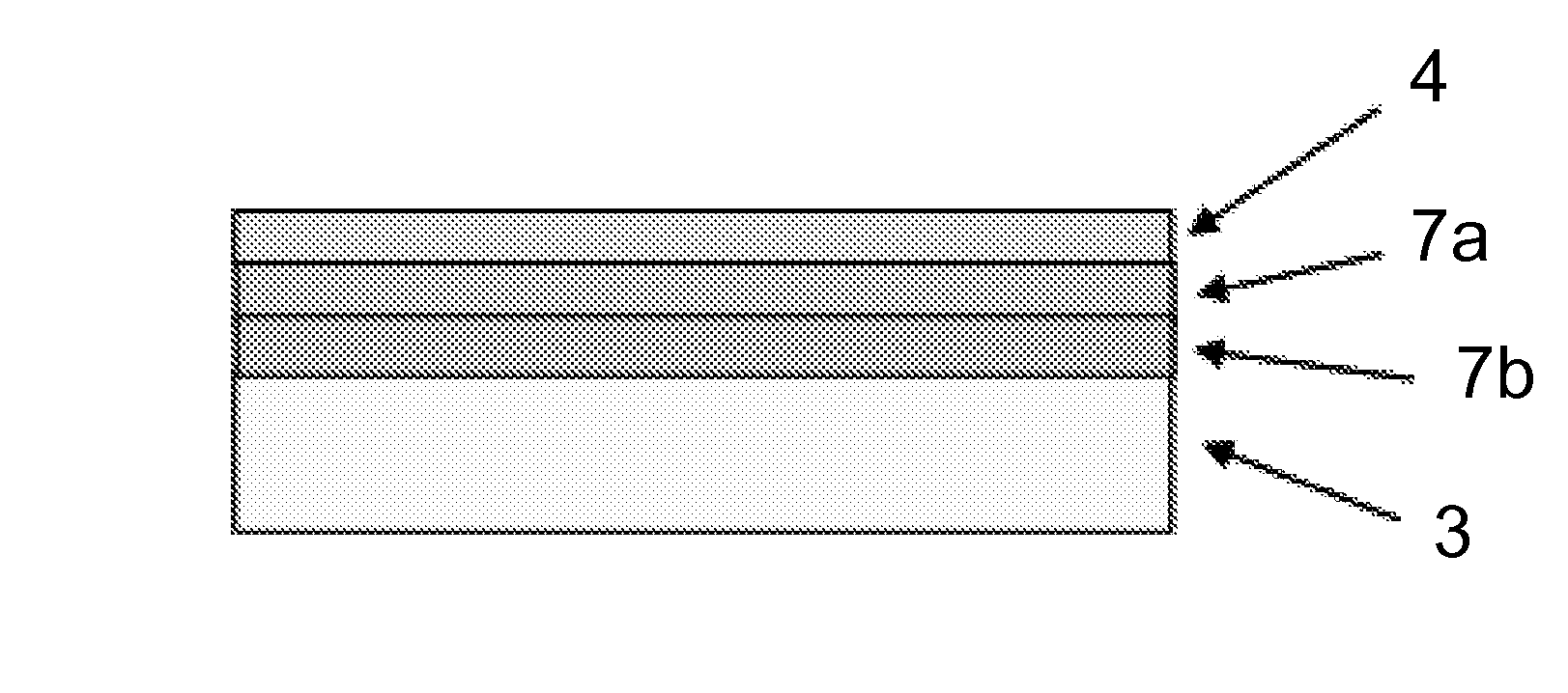
[0044]Commonly used support substrates are advantageously entirely made of glass, and their thickness lies between 500 μm and 750 μm according to their application, while the transferred single crystalline layer 4 has a thickness varying between 0.01 μm to 2 μm.

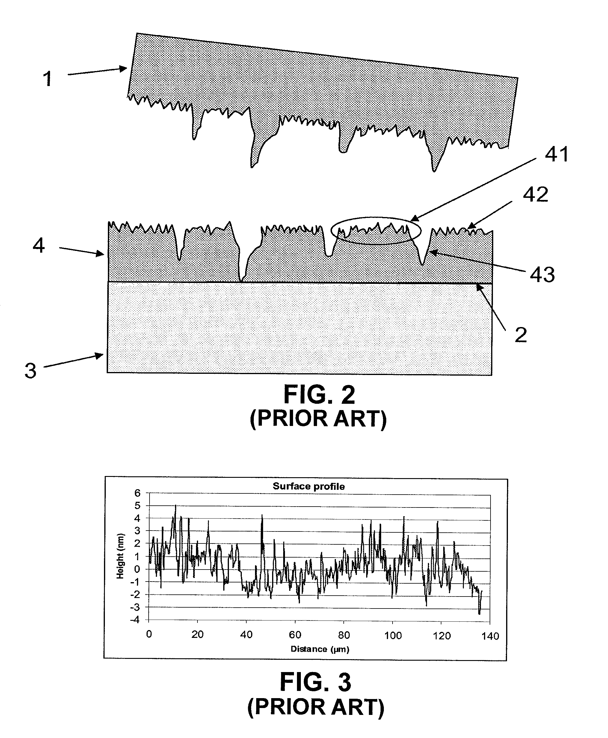
[0045]The applicant has surprisingly discovered that the thickness of the glass-based support substrate 3 appears to have an impact on the density and the depth of surface irregularities at the separation zone 2 of the source substrate 1.

[0046]In this respect, FIGS. 4a and 4b are optical profilometry images representing the surface of a sil...


PUM


Abstract

A method for reducing irregularities at a surface of a layer transferred from a source substrate to a glass-based support substrate, by generating a weakening zone in the source substrate; contacting the source substrate and the glass-based support substrate; and splitting the source substrate at the weakening zone; wherein the glass-based substrate has a thickness of between 300 μm and 600 μm.

Description

FIELD OF THE INVENTION[0001]The field of this invention is that of Silicon On Glass (SiOG) structures.[0002]More precisely, the invention relates to an improved method for making such structures.BACKGROUND OF THE INVENTION[0003]Silicon On Insulator (SOI) technology is becoming increasingly important for high performance thin film transistors, solar cells, etc. SOI wafers consist of a thin layer of substantially single crystal silicon (generally less than one micron) on an insulating material.[0004]Various structures and various ways of obtaining such wafers are known. Typically, used structures are formed with a thin film of single crystalline silicon 0.01-2 μm in thickness bonded to another silicon wafer with an oxide insulator layer in between.[0005]Because of its rather high thickness, in particular as compared to the other parts, a major fraction of the cost of such structures has been the cost of the silicon substrate that supports the oxide layer, topped by the thin silicon la...

Claims


Application Information

Patent Timeline
Patent Type & Authority Patents(United States)
IPC IPC(8): H01L21/30H01L21/18H01L21/762H01L29/02
CPCH01L29/02H01L21/76254H01L21/185H01L21/762H01L21/20H01L21/761
Inventor DELPRAT, DANIELDURET, CARINEBEN-MOHAMED, NADIALALLEMENT, FABRICE
Owner SOITEC SA
Why Eureka
Try Eureka