

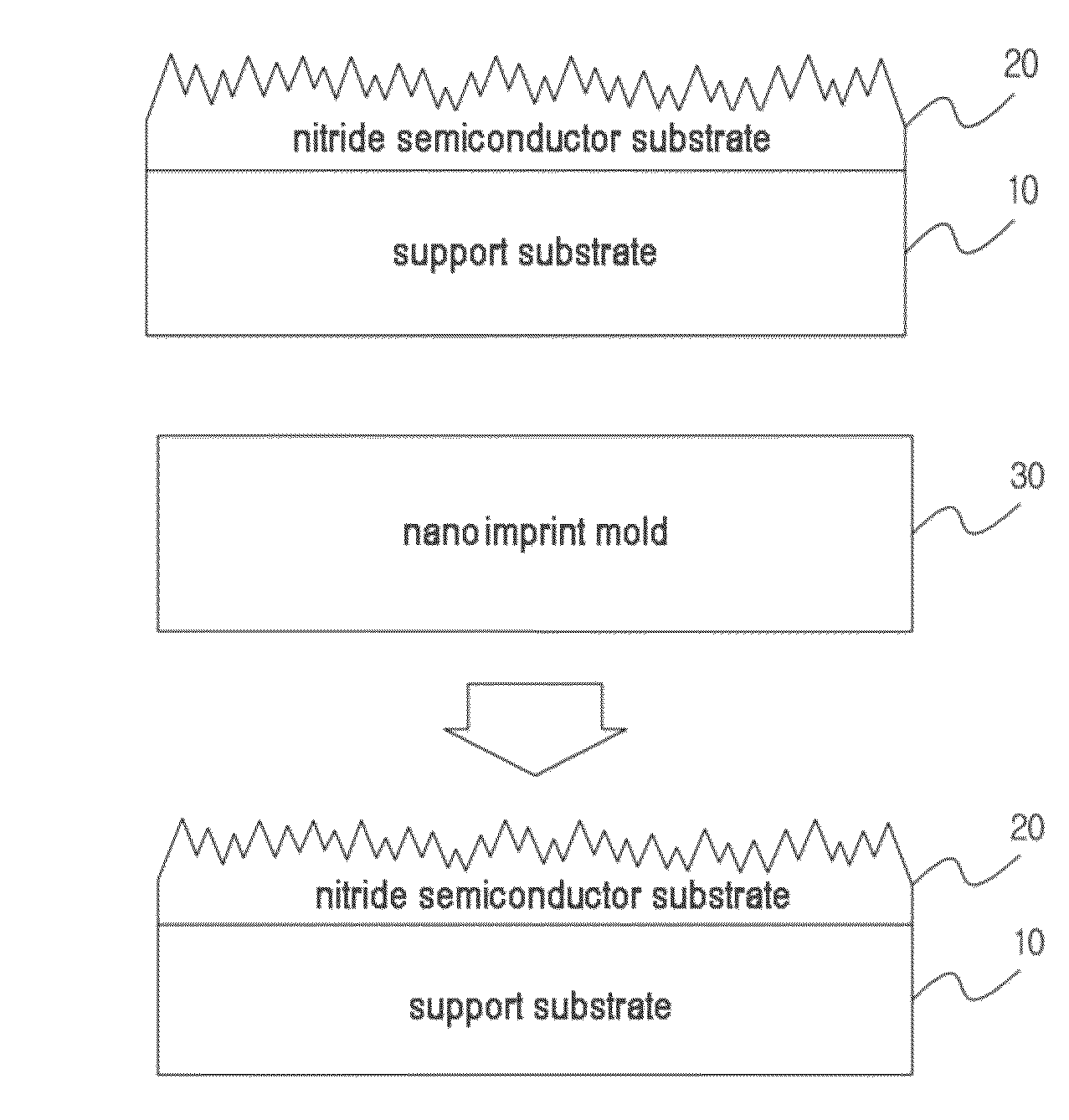
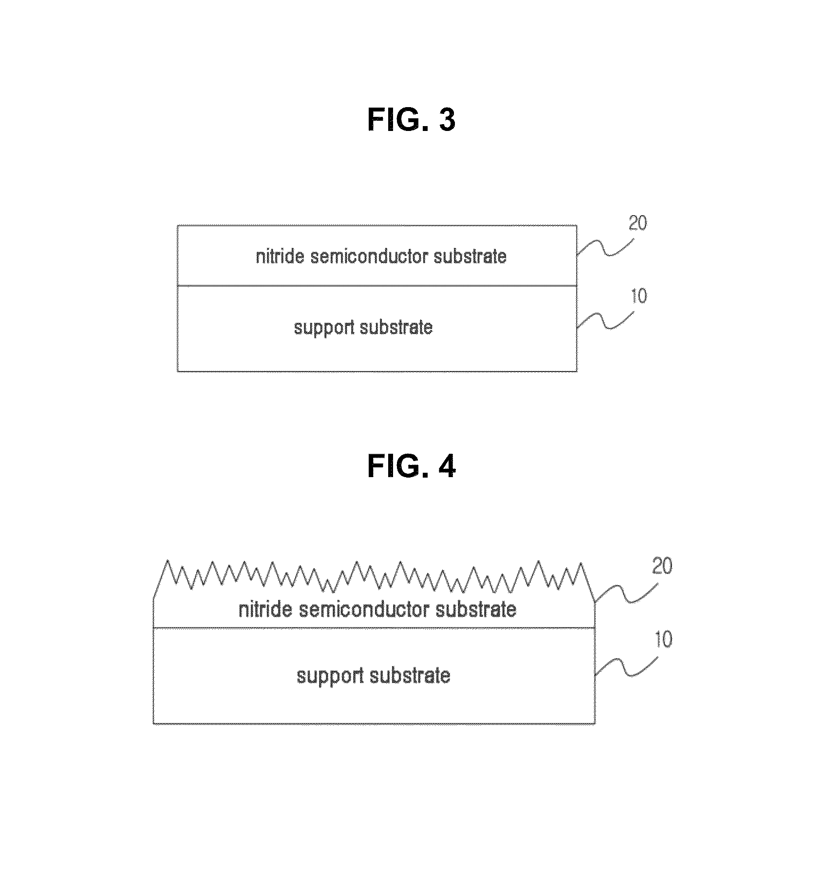
Method of fabricating nano-imprint mold for a light emitting diode
a technology of light-emitting diodes and nano-imprint molds, which is applied in the field of manufacturing nano-imprint molds, can solve the problems of difficult to form uniform nano structures in a large area, and cannot be used as outdoor light sources, so as to improve the light extraction efficiency of light-emitting diodes, efficiently and precisely form nano-patterns, and achieve efficient and economical formation
- Summary
- Abstract
- Description
- Claims
- Application Information
AI Technical Summary
Benefits of technology
Problems solved by technology
Method used
Image

Examples
first embodiment
[0050]FIGS. 10 to 18 are views illustrating a method of manufacturing a light emitting diode according to the present invention.
[0051]Referring to FIGS. 10 to 18, a method of manufacturing a light emitting diode according to a first embodiment of the present invention includes a process of forming an n-type nitride semiconductor layer 110, a light-emitting layer 120, and a p-type nitride semiconductor layer 130 on a temporary substrate 100, a process of forming a p-type electrode 140 on the p-type nitride semiconductor layer 130, a process of forming a conductive substrate 150 on the p-type electrode 140, a process of exposing the n-type nitride semiconductor layer 110 by removing the n-type nitride semiconductor layer 110, a process of forming a nanoimprint resist layer 160 on the n-type nitride semiconductor layer 110, a process for transferring a nano-pattern transferred onto the nanoimprint resist layer 160 by pressing a nanoimprint mold 30 that is formed by the method of manufa...
second embodiment
[0069]FIGS. 19 to 25 are views illustrating a method of manufacturing a light emitting diode according to the present invention.
[0070]Referring to FIGS. 19 to 25, a method of manufacturing a light emitting diode according to a second embodiment includes a process of forming an n-type nitride semiconductor layer 210, a light-emitting layer 220, and a p-type nitride semiconductor layer 230 on a semiconductor substrate 200 having a pattern for reflecting light through scattering, a process of exposing a portion of the n-type nitride semiconductor layer 210 by mesa-etching a portion of the p-type nitride semiconductor layer 230, the light-emitting layer 220, and the p-type nitride semiconductor layer 230, a process of forming a transparent electrode layer 240 on the p-type nitride semiconductor layer 230, a process of forming a nanoimprint resist layer 250 on the transparent electrode layer 240, a process of transferring a nano-pattern transferred onto a nanoimprint resist layer 250 by ...
PUM
| Property | Measurement | Unit |
|---|---|---|
| refractive index | aaaaa | aaaaa |
| critical angle | aaaaa | aaaaa |
| refractive index | aaaaa | aaaaa |
Abstract
Description
Claims
Application Information