

Method for manufacturing nano-imprint mould, method for manufacturing light-emitting diode using the nano imprint mould manufactured thereby, and light-emitting diode manufactured thereby
a nano-imprint mold and manufacturing method technology, applied in the field of nano-imprint mold manufacturing, can solve the problems of inability to adapt to use as an outdoor light source, reproducibility may be deteriorated, manufacturing costs may be increased, etc., to achieve efficient and economical formation, enhance the light extraction efficiency of light emitting diodes, and efficiently and precisely form nano-patterns
- Summary
- Abstract
- Description
- Claims
- Application Information
AI Technical Summary
Benefits of technology
Problems solved by technology
Method used
Image

Examples
Embodiment Construction
[0070]FIGS. 19 to 25 are views illustrating a method of manufacturing a light emitting diode according to a second embodiment of the present invention.
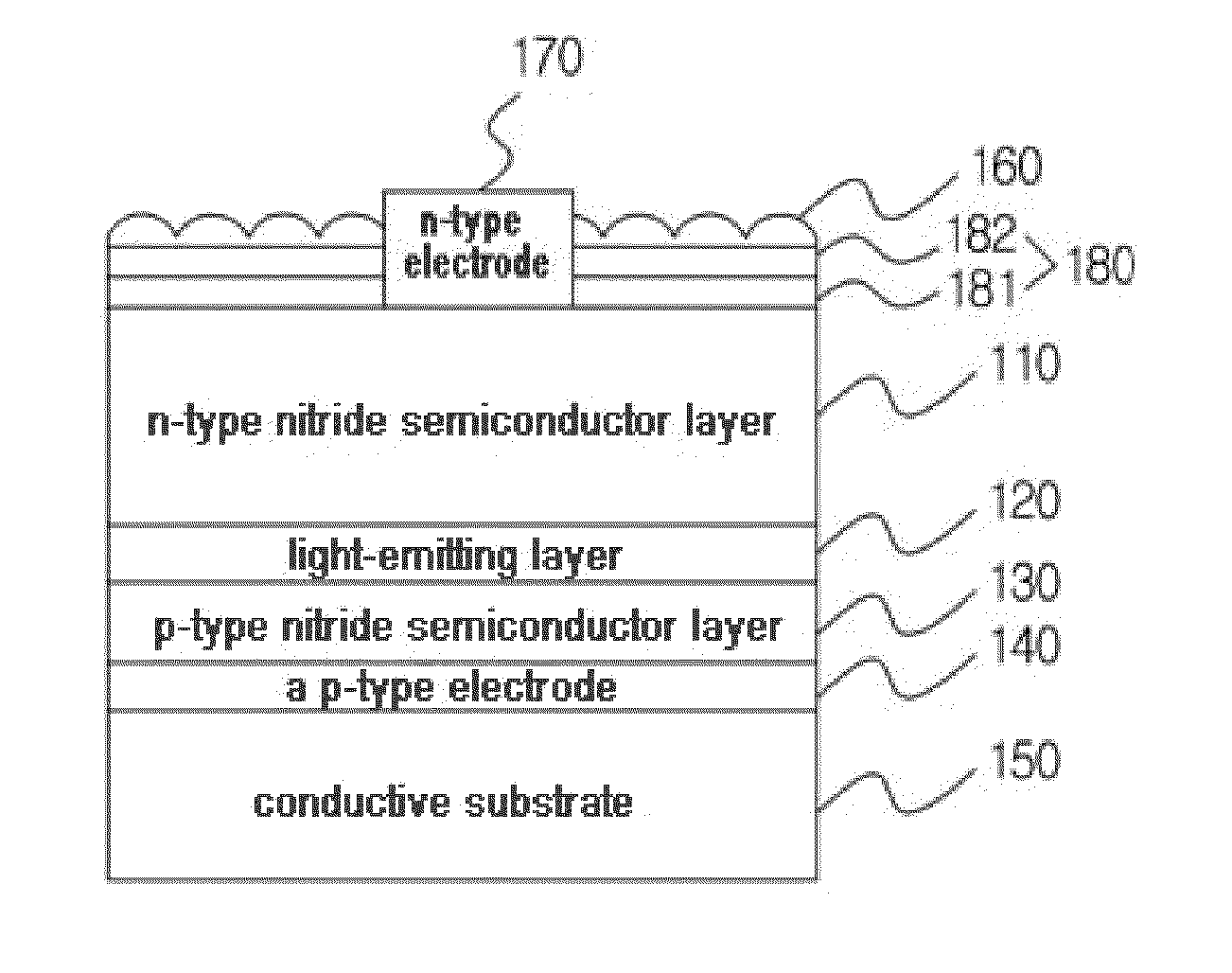
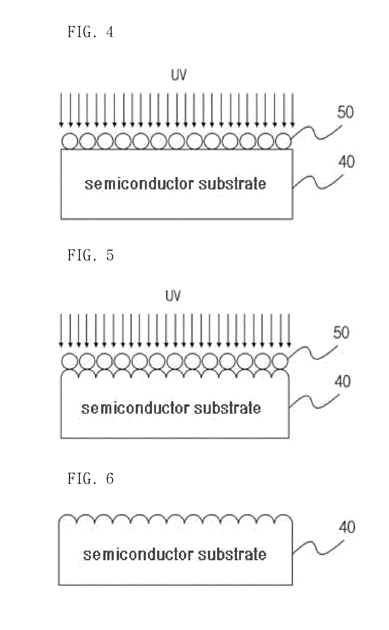
[0071]Referring to FIGS. 19 to 25, a method of manufacturing a light emitting diode according to a second embodiment includes a process of forming an n-type nitride semiconductor layer 210, a light-emitting layer 220, and a p-type nitride semiconductor layer 230 on a semiconductor substrate 200 having a pattern for reflecting light through scattering, a process of exposing a portion of the n-type nitride semiconductor layer 210 by mesa-etching a portion of the p-type nitride semiconductor layer 230, the light-emitting layer 220, and the p-type nitride semiconductor layer 230, a process of forming a transparent electrode layer 240 on the p-type nitride semiconductor layer 230, a process of forming a nanoimprint resist layer 250 on the transparent electrode layer 240, a process of transferring a nano-pattern transferred onto a nanoimpri...
PUM
| Property | Measurement | Unit |
|---|---|---|
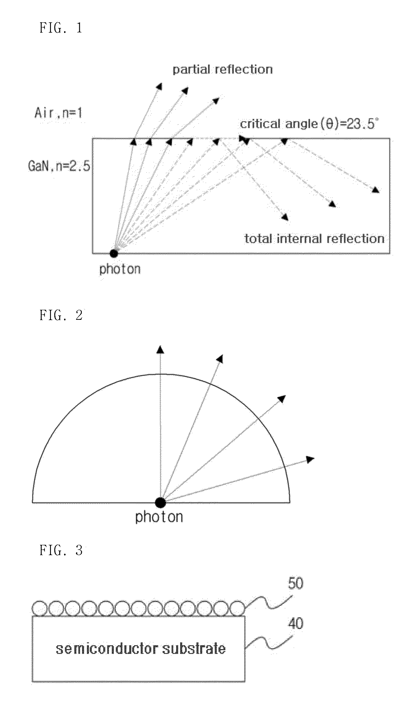
| refractive index | aaaaa | aaaaa |
| size | aaaaa | aaaaa |
| critical angle | aaaaa | aaaaa |
Abstract
Description
Claims
Application Information