Mounted structure

a technology of mounted structures and mounting plates, applied in the field of electronic packaging, can solve the problems of reducing the ductility of the mounted layers, generating cracks in the power semiconductor elements, and unable to relax electrodes, so as to prevent the crack generation of the semiconductor elements or peeling, prevent the crack generation of the semiconductor elements, and ensure the effect of ductility

Inactive Publication Date: 2015-02-17
PANASONIC INTELLECTUAL PROPERTY MANAGEMENT CO LTD
View PDF14 Cites 0 Cited by
  • Summary
  • Abstract
  • Description
  • Claims
  • Application Information

AI Technical Summary

Benefits of technology

[0011]Thus, it is an object of the present invention to provide a mounted structure of a power semiconductor module capable of showing heat resistance to heat generation of a power semiconductor element, and preventing peeling between a mounted layers and the power semiconductor element.
[0022]As described above, according to the mounted structure in the present invention, the mounted layers for bonding the electrode of the substrate and the electrode of the semiconductor element includes the first intermetallic compound layer containing the CuSn-based intermetallic compound, the Bi layer, the second intermetallic compound layer containing the CuSn-based intermetallic compound, the Cu layer, and the third intermetallic compound layer containing the CuSn-based intermetallic compound which are sequentially arranged from the electrode of the substrate toward the electrode of the semiconductor element. When the semiconductor element and the electrode of the substrate are bonded through this mounted layers, a stress can be relaxed by ductility of the Cu layer and low elasticity (32×109, N / m2) of the Bi layer, with respect to the thermal stress in the bonding process, so that it is possible to prevent the crack generation of the semiconductor element, or the peeling between the semiconductor element and the mounted layers.
[0023]In addition, the intermetallic compound layers, the Cu layer, and the Bi layer composing the mounted layers each have sufficient heat resistance, so that it is possible to ensure the heat resistance to heat generation of the semiconductor element at the time of an operation of the power semiconductor module. As a result, the mounted structure in the present invention can achieve both of the prevention of the crack generation of the semiconductor element or the peeling between the semiconductor element and the mounted layers due to the thermal stress, and the heat resistance, in the bonding process. Thus, the semiconductor element and the electrode can be bonded with high quality to improve bonding reliability.

Problems solved by technology

However, crack may be generated in the power semiconductor element, or an interface between the power semiconductor element and the mounted layers may be peeled off at the time of cooling down from 260° C. heated in a bonding process to room temperature.
It is considered that this is because ductility of the mounted layers is lost due to the intermetallic compound of Sn and Ag, or Sn and Cu, and the thermal stress caused by a linear expansion coefficient difference between the power semiconductor element and the electrode cannot be relaxed in the bonding process of the power semiconductor element.

Method used


Image

  • Mounted structure
  • Mounted structure
  • Mounted structure

Examples


first embodiment

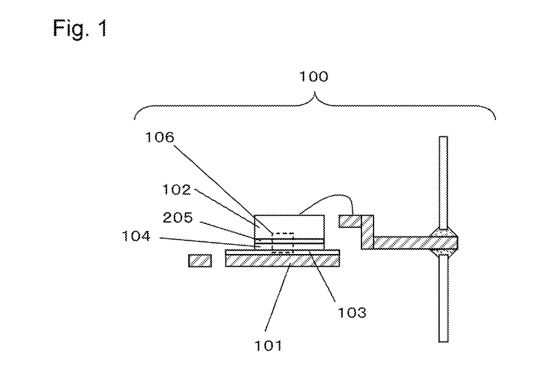
[0068]FIG. 1 is a cross-sectional view of a power semiconductor module 100 bonded with a mounted layers 104 according to a first embodiment. This power semiconductor module 100 includes a substrate 101, and a semiconductor element 102 bonded to an electrode 103 provided on the substrate 101 through the mounted layers 104. In addition, a mounted structure 106 includes an electrode 205 of the semiconductor element 102, the mounted layers 104, and the electrode 103.

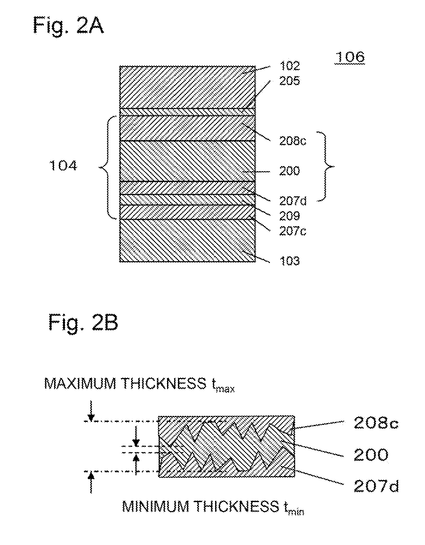
[0069]Next, this formed mounted structure 106 will be described in detail with reference to FIG. 2A and FIG. 2B, FIG. 2A is a cross-sectional view showing a detailed cross-sectional structure of the mounted structure 106. This mounted structure 106 includes the electrode 103, the electrode 205 of the semiconductor element 102, and the mounted layers 104 for bonding the electrode 103 and the electrode 205. The mounted layers 104 is provided in such a manner that a first intermetallic compound layer 207c containing a CuSn-base...

second embodiment

[0104]FIG. 5A is a cross-sectional view showing a detailed cross-sectional structure of a mounted structure 106 according to a second embodiment. FIG. 5B is an enlarged cross-sectional view of a Cu layer 200 in FIG. 5A. FIGS. 6A to 6C are flowcharts of manufacturing steps of the mounted structure according to the second embodiment.

[0105]As shown in FIG. 5A, the mounted structure 106 according to the second embodiment includes an electrode 103, an electrode 205 of a semiconductor element 102, and a mounted layers 104 provided between them. As shown in the cross-sectional view in FIG. 6A, compared with the bonding material according to the first embodiment, a bonding material 213 used in the second embodiment is different in that an Sn—Bi layer 204 and an Sn layer 206 are arranged so as to be vertically reversed across the Cu layer 200, between the electrode 103 side and the electrode 205 of the semiconductor element 102. As a result, as shown in FIG. 5A, the formed mounted layers 104...

third embodiment

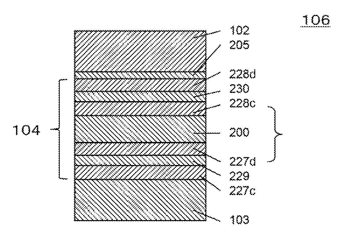
[0110]FIG. 7A is a cross-sectional view showing a detailed cross-sectional structure of a mounted structure 106 according to a third embodiment. This mounted structure 106 includes an electrode 103, an electrode 205 of a semiconductor element 102, and a mounted layers 104 for bonding the electrode 103 and the electrode 205. The mounted layers 104 includes a first intermetallic compound layer 227c containing a CuSn-based intermetallic compound, a Bi layer 229, a second intermetallic compound layer 227d containing a CuSn-based intermetallic compound, a Cu layer 200, a third intermetallic compound layer 228c containing a CuSn-based intermetallic compound, a Bi layer 230, and a fourth intermetallic compound layer 228d containing a CuSn-based intermetallic compound. The above layers are sequentially arranged from a side of the electrode 103 toward a side of the electrode 205 of the semiconductor element 102 to configure the mounted layers 104. In addition, FIG. 7B is an enlarged cross-se...


PUM

PropertyMeasurementUnit
thicknessaaaaaaaaaa
areaaaaaaaaaaa
areaaaaaaaaaaa

Abstract

A mounted structure includes an electrode of a substrate, an electrode of a semiconductor element, and a mounted layers for bonding the electrode of the substrate and the electrode of the semiconductor element, and the mounted layers includes: a first intermetallic compound layer containing a CuSn-based intermetallic compound; a Bi layer; a second intermetallic compound layer containing a CuSn-based intermetallic compound; a Cu layer; and a third intermetallic compound layer containing a CuSn-based intermetallic compound, and the above layers are sequentially arranged from the electrode of the substrate toward the electrode of the semiconductor element to configure the mounted layers.

Description

TECHNICAL HELD[0001]The present invention relates to an internal bonding of a semiconductor component. More particularly, the present invention relates to a mounted structure including a mounted layers for bonding an electrode of a semiconductor element and an electrode of a substrate in a power semiconductor module required to have superior mechanical characteristics and heat resistance.DESCRIPTION OF THE RELATED ART[0002]In an electronics packaging field, out of a concern of harm of lead and an increasing interest about the environment, a bonding desirably does not use lead. Then, as for a Sn—Pb eutectic solder which is a general solder material its alternative material has been developed and practically used.[0003]Meanwhile, in the context of technical development of GaN and SiC serving as a next-generation high output device as alternatives to conventional Si, a Pb-free solder material having high heat resistance to a device heat generation temperature of 250° C. has been studie...

Claims


Application Information

Patent Timeline
Patent Type & Authority Patents(United States)
IPC IPC(8): H01L23/12H01L23/52H01L29/40B23K35/02B23K35/22B23K35/26B23K35/30H01L23/00H01L23/488H01L23/492H01L23/495
CPCH01L24/05B23K35/0272B23K35/22H01L24/29H01L24/83H01L24/32H01L23/488H01L23/492B23K35/264B23K35/302B23K35/0261H01L2224/32245H01L2224/48091H01L2224/48247H01L2224/73265H01L2224/83101H01L24/48H01L2924/01327H01L2924/01322H01L2924/3025H01L23/49513H01L2224/04026H01L2224/05639H01L2224/05644H01L2224/05647H01L2224/05655H01L2224/29083H01L2224/29111H01L2224/29139H01L2224/29147H01L2224/83192H01L2224/83439H01L2224/83447H01L2224/8381H01L2924/00014H01L2924/00012H01L2924/00H01L2224/45099H01L2924/01083H01L2224/04042H01L2224/27334H01L2224/83411H01L2224/05611H01L2224/2712H01L2224/32503H01L2224/32507H01L2224/83065H01L2224/83201H01L2224/83444H01L2224/83455H01L2224/83986H01L2924/351H01L2924/3512H01L2924/35121H01L2924/203H01L2924/12042H01L24/73H01L2224/8321H01L2924/0002
Inventor NAKAMURA, TAICHIKITAURA, HIDETOSHI
Owner PANASONIC INTELLECTUAL PROPERTY MANAGEMENT CO LTD
Why Eureka
Try Eureka