Liquid crystal display device
a liquid crystal display and display screen technology, applied in non-linear optics, instruments, optics, etc., can solve problems such as bright spots, and achieve the effects of preventing the generation of bright spots, reducing the gap between the column spacer and the tft substrate, and suppressing the peeling of the alignment film
- Summary
- Abstract
- Description
- Claims
- Application Information
AI Technical Summary
Benefits of technology
Problems solved by technology
Method used
Image
Examples
first embodiment
[First Embodiment]
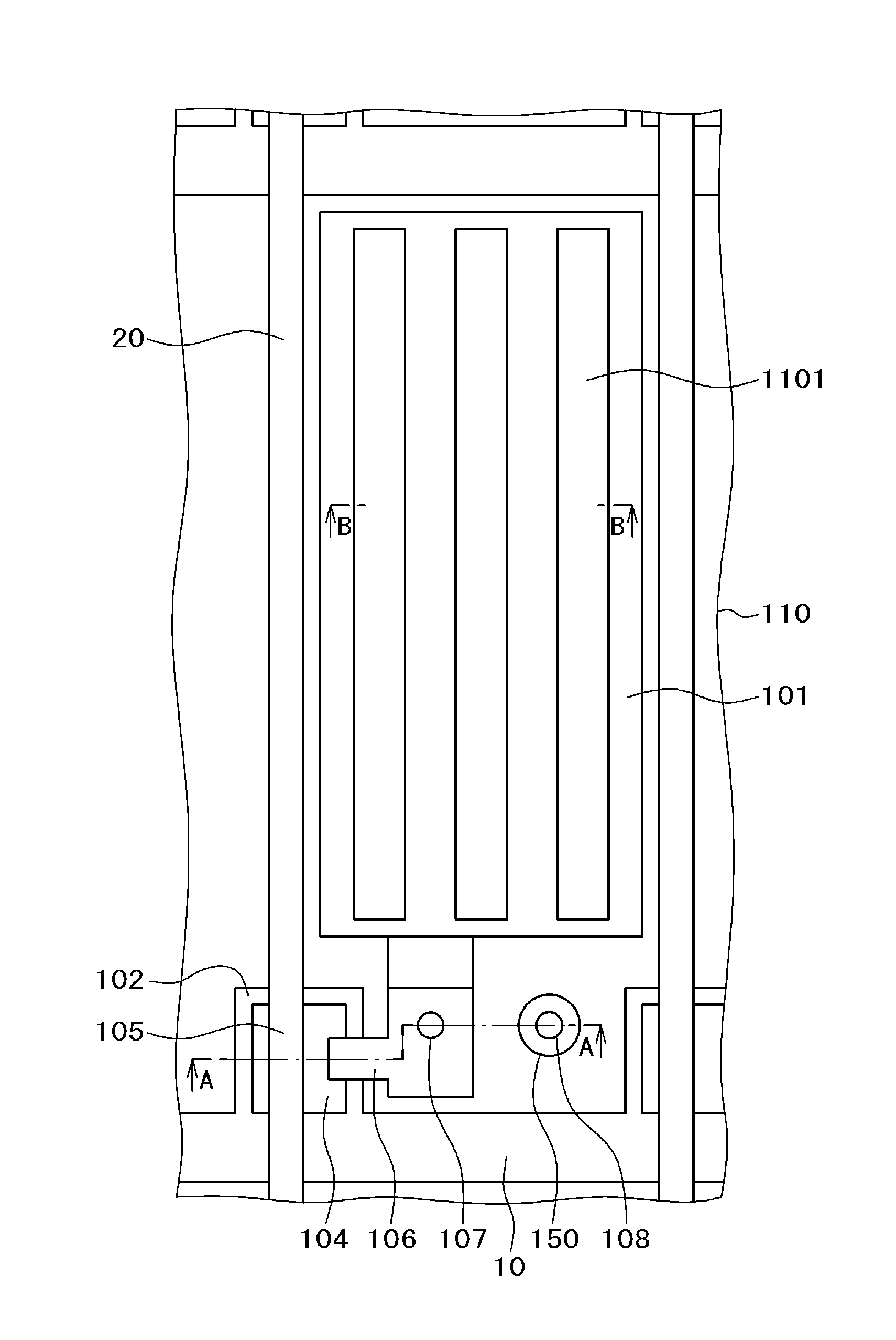
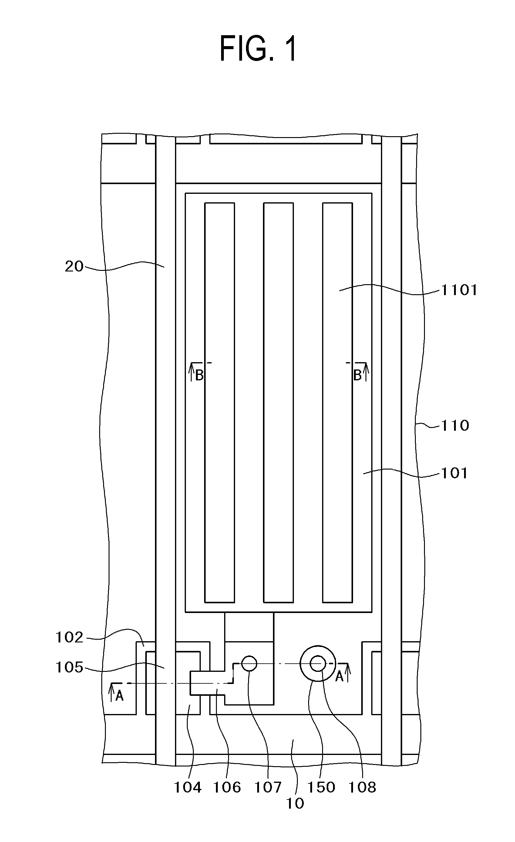
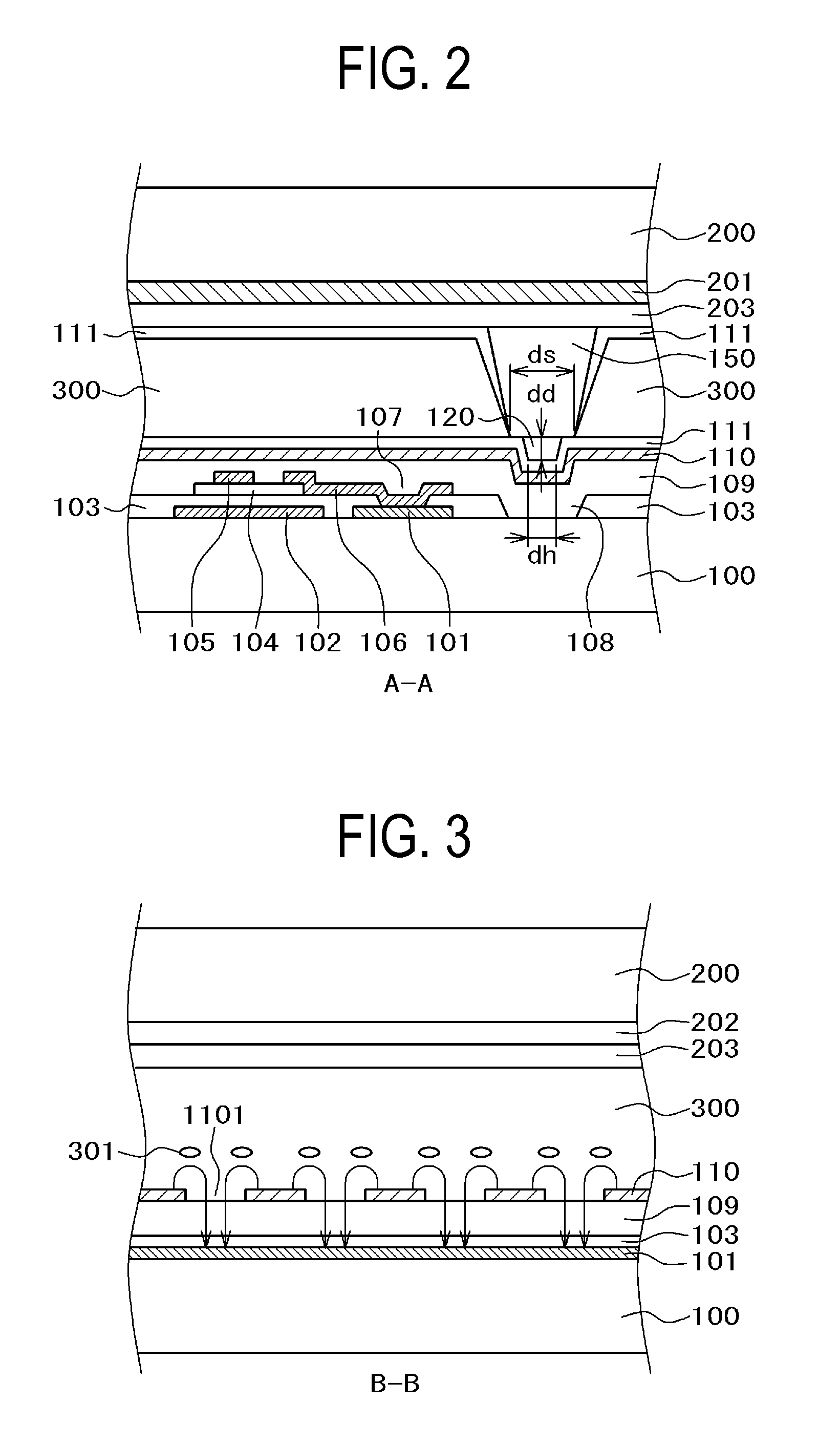
[0040]FIG. 1 is a plan view for a pixel portion of a liquid crystal display device to which the present invention is applied, FIG. 2 is a cross sectional view along line A-A in FIG. 1, and FIG. 3 is a cross sectional view along a line B-B in FIG. 1. In FIG. 1, gate lines 10 are extended in a lateral direction and arranged in a longitudinal direction. Further, the data lines 20 are extended in the longitudinal direction and arranged in the lateral direction. A pixel electrode 101 is formed in a region surrounded by the gate lines 10 and the data lines 20. The pixel electrode 101 is formed as a solid plane, on which a gate insulating film and an inorganic passivation film not illustrated in FIG. 1 are stacked, and a counter electrode 110 having slits 1101 is arranged thereover. The counter electrode 110 is formed in common with each of the pixels.
[0041]FIG. 3 is a cross sectional view along line B-B in FIG. 1 showing the configuration described above. In FIG. 3, a pi...
second embodiment
[Second Embodiment]
[0057]FIG. 4 is a plan view showing a second embodiment of the invention. In FIG. 4, compared with FIG. 1 of the first embodiment, a source electrode 106 is extended longer in the right direction and formed as far as the through hole 108 in the gate insulating film 103 formed corresponding to the columnar spacer 150. Other configurations in FIG. 4 are identical with those of FIG. 1.
[0058]FIG. 5 is a cross sectional view along line C-C in FIG. 4. FIG. 4 is different from FIG. 2 for the first embodiment in that a source electrode 106 is extended covering the portion of the through hole 108 in the gate insulating film 103 which is formed corresponding to the columnar spacer 150. In the configuration of FIG. 5, the source electrode 106 and an inorganic passivation film 109 are present in the through hole 108 which is formed in the gate insulating film 103. Presence or absence of the source electrode 106 formed in the through hole portion 108 can be utilized for contro...
third embodiment
[Third Embodiment]
[0059]FIG. 6 is a plan view showing a third embodiment of the invention. In FIG. 6, compared with FIG. 1 for the first embodiment, a source electrode 106 is extended in the right direction and is formed as far as the end of a through hole 108 in a gate insulation film 103 formed corresponding to a columnar spacer 150, and a metal film formed simultaneously with the source electrode 106 is formed also on the side opposite to the through hole 108. However, the source electrode 106 is not formed inside the through hole 108.
[0060]FIG. 7 is a cross sectional view along line D-D in FIG. 6. FIG. 7 is different from FIG. 2 of the first embodiment in that the source electrode 106 is formed as far as the end of the through hole 108, and a metal film formed simultaneously with the source electrode 106 is formed at the surface of the gate insulating film 103 on the other side of the through hole 108. As shown in FIG. 7, the gate electrode 106 is not formed inside the through h...
PUM
| Property | Measurement | Unit |
|---|---|---|
| thickness | aaaaa | aaaaa |
| depth dd | aaaaa | aaaaa |
| depth dd | aaaaa | aaaaa |
Abstract
Description
Claims
Application Information
 - R&D
- Intellectual Property
- Life Sciences
- Materials
- Tech Scout
- Unparalleled Data Quality
- Higher Quality Content
- 60% Fewer Hallucinations
Browse by: Latest US Patents, China's latest patents, Technical Efficacy Thesaurus, Application Domain, Technology Topic, Popular Technical Reports.
© 2025 PatSnap. All rights reserved.Legal|Privacy policy|Modern Slavery Act Transparency Statement|Sitemap|About US| Contact US: help@patsnap.com


