

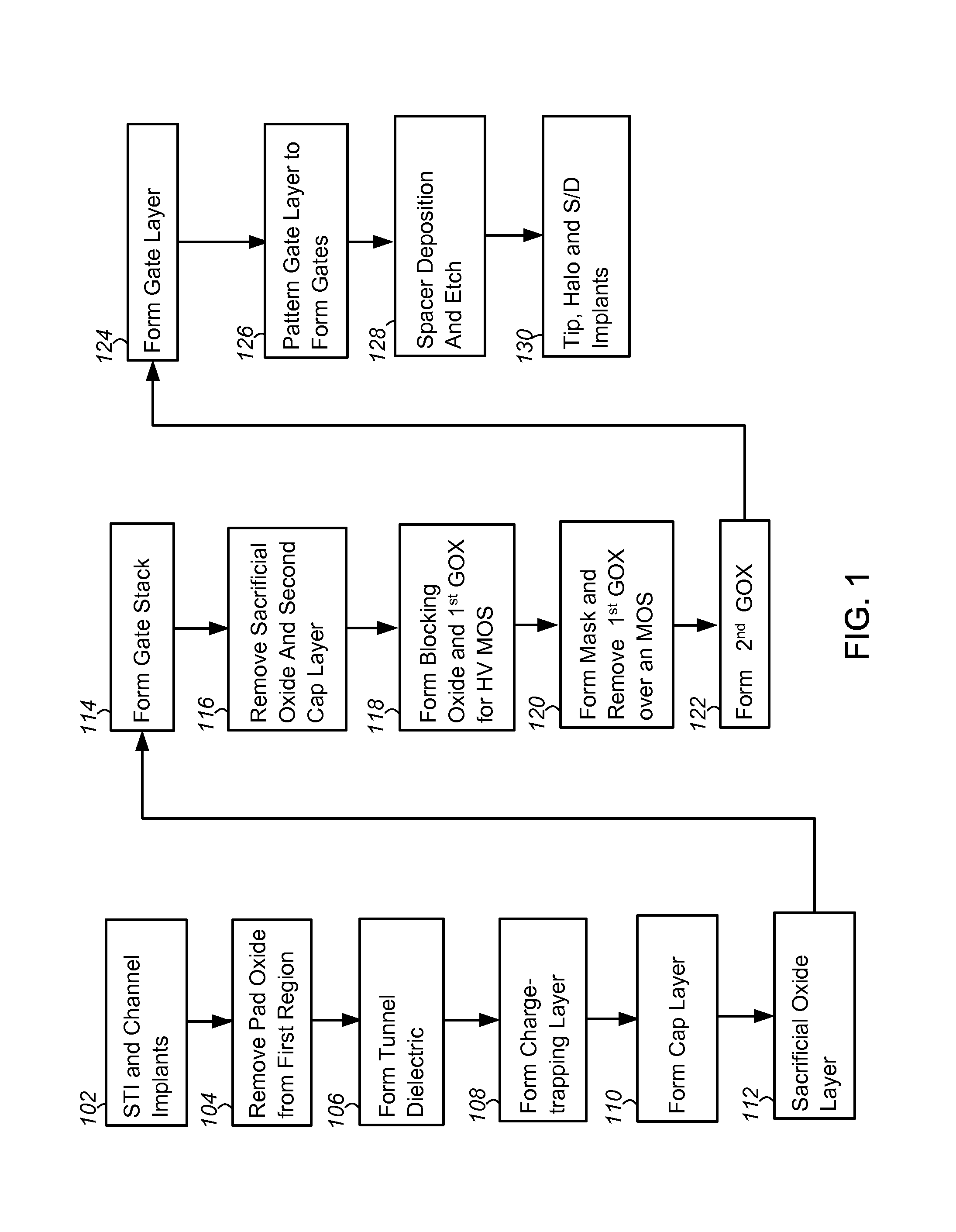
Method of fabricating a charge-trapping gate stack using a CMOS process flow
a charge-trapping gate and process flow technology, applied in the field of semiconductor devices, can solve the problems of affecting affecting the fabrication of mosfets, and significantly degrading the performance of a previously formed ono stack
- Summary
- Abstract
- Description
- Claims
- Application Information
AI Technical Summary
Benefits of technology
Problems solved by technology
Method used
Image

Examples
Embodiment Construction
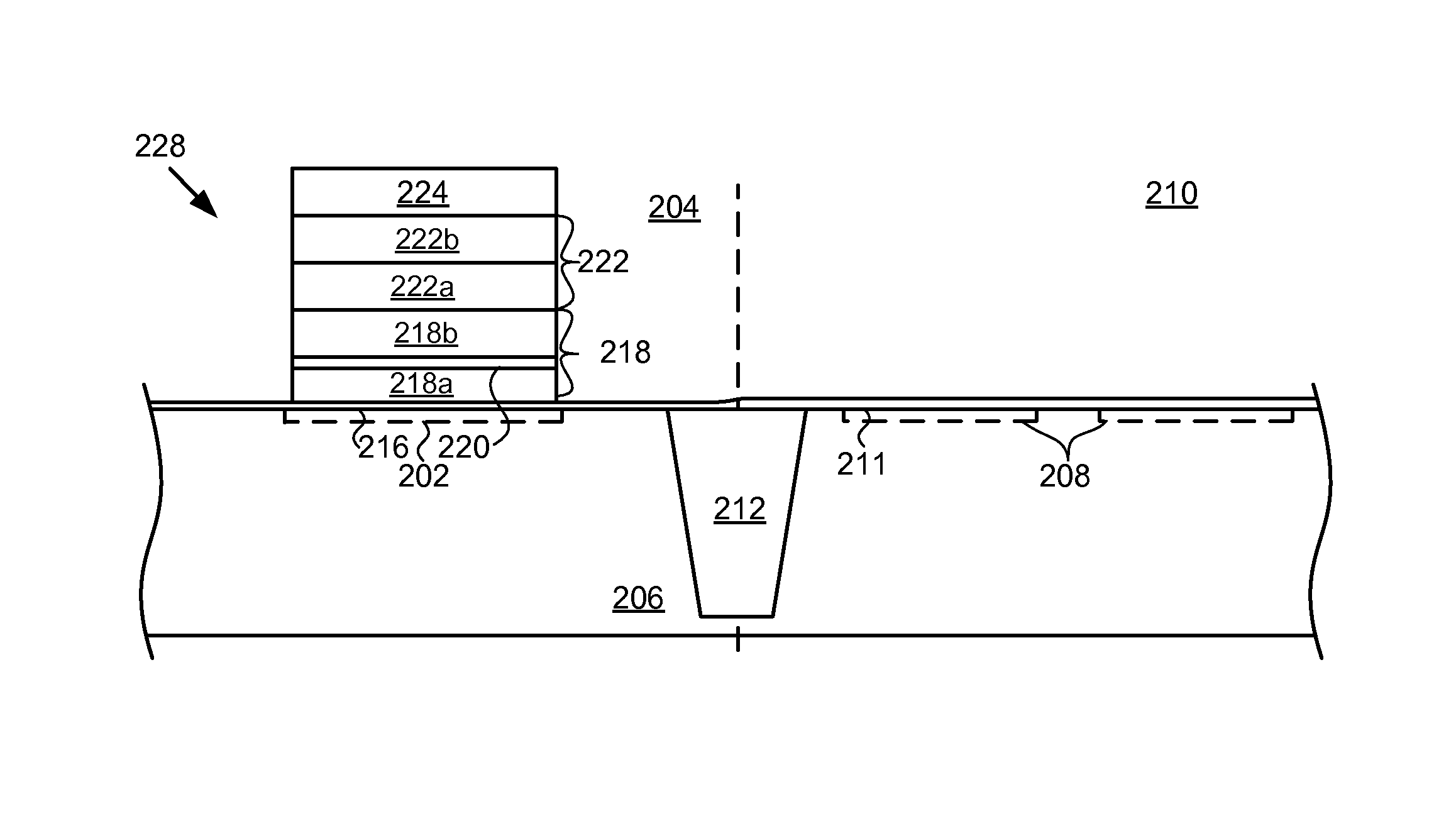
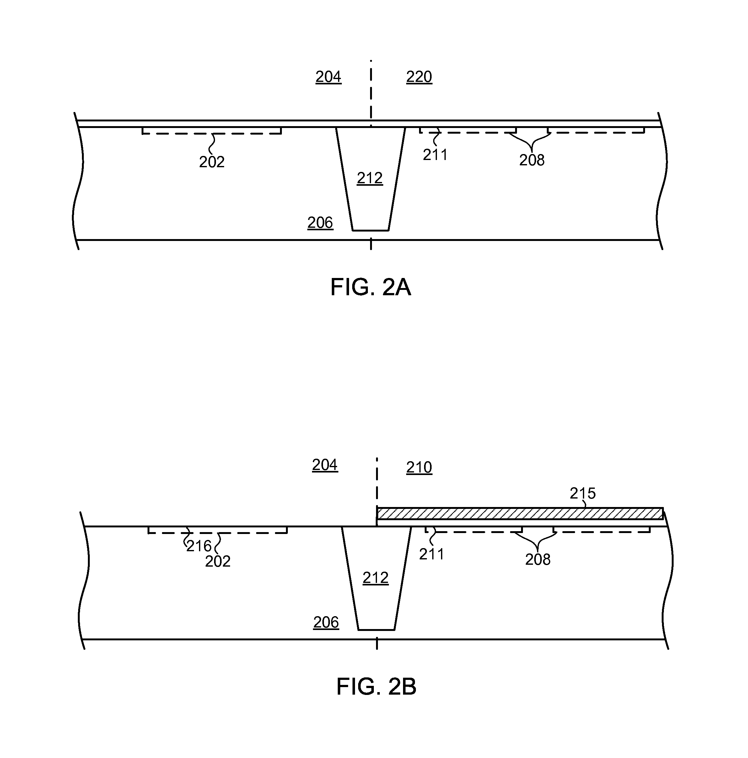
[0012]The present disclosure is directed generally to a method of integrating a memory device including a charge-trapping gate stack into a CMOS process flow.
[0013]In the following description, numerous specific details are set forth, such as specific configurations, compositions, and processes, etc., in order to provide a thorough understanding of the present invention. In other instances, well-known processes and manufacturing techniques have not been described in particular detail in order to not unnecessarily obscure the present invention. Furthermore, it is to be understood that the various embodiments shown in the Figures are illustrative representations and are not necessarily drawn to scale.
[0014]The terms “above,”“over,”“between,” and “on” as used herein refer to a relative position of one layer with respect to other layers. One layer deposited or disposed above or under another layer may be directly in contact with the other layer or may have one or more intervening layers...
PUM
| Property | Measurement | Unit |
|---|---|---|
| thickness | aaaaa | aaaaa |
| pressure | aaaaa | aaaaa |
| thickness | aaaaa | aaaaa |
Abstract
Description
Claims
Application Information