EMI-preventing socket and manufacturing method thereof

a manufacturing method and technology of emi, applied in the direction of coupling device details, coupling device connection, coupling protective earth/shielding arrangement, etc., can solve the problems of reducing the performance of devices, apparatuses or systems, damage to lives or inorganic materials, radiation may be easily leaked from the transmitting medium, etc., to achieve the effect of effective prevention of emi, improving the assembling process, and enhancing production performan

Active Publication Date: 2015-04-07
DELTA ELECTRONICS (SHANGHAI) CO LTD +1
View PDF26 Cites 8 Cited by
  • Summary
  • Abstract
  • Description
  • Claims
  • Application Information

AI Technical Summary

Benefits of technology

[0008]In view of the foregoing, the present invention is to provide a manufacturing method of an EMI-preventing socket that can effectively prevent the EMI, improve the assembling process, and enhance the production performance.
[0016]As mentioned above, the manufacturing method of the present invention is to connect the EMI-preventing element with the ground pin in advance by, for example, riveting, and then form the socket body of the EMI-preventing socket by injection molding. In other words, the EMI-preventing element and the ground pin are connected before injecting the molding material. This procedure can firmly connect the EMI-preventing element with the ground pin. After the following molding step, the manufactured product can effectively prevent the undesired EMI, increase the production yield, and reduce the manufacturing time. Besides, the manufacturing method of the present invention does not use a soldering process to connect the EMI-preventing element with the ground pin, so that it can reduce manpower cost and working time and be more environmentally friendly.

Problems solved by technology

Electromagnetic interference (EMI) may decrease the performance of devices, apparatuses or systems, or cause harmful electromagnetic results which damage lives or inorganic materials.
If high-frequency wave energy and signal modulation are used, the radiation may be easily leaked from the transmitting medium.
However, the soldering process for connecting the conductive element 12 and the ground pin 111 easily affects the stability of the manufacturing processes and needs longer working time, so it is not suitable for mass production and rework.

Method used


Image

  • EMI-preventing socket and manufacturing method thereof
  • EMI-preventing socket and manufacturing method thereof
  • EMI-preventing socket and manufacturing method thereof

Examples


Embodiment Construction

[0021]The present invention will be apparent from the following detailed description, which proceeds with reference to the accompanying drawings, wherein the same references relate to the same elements.

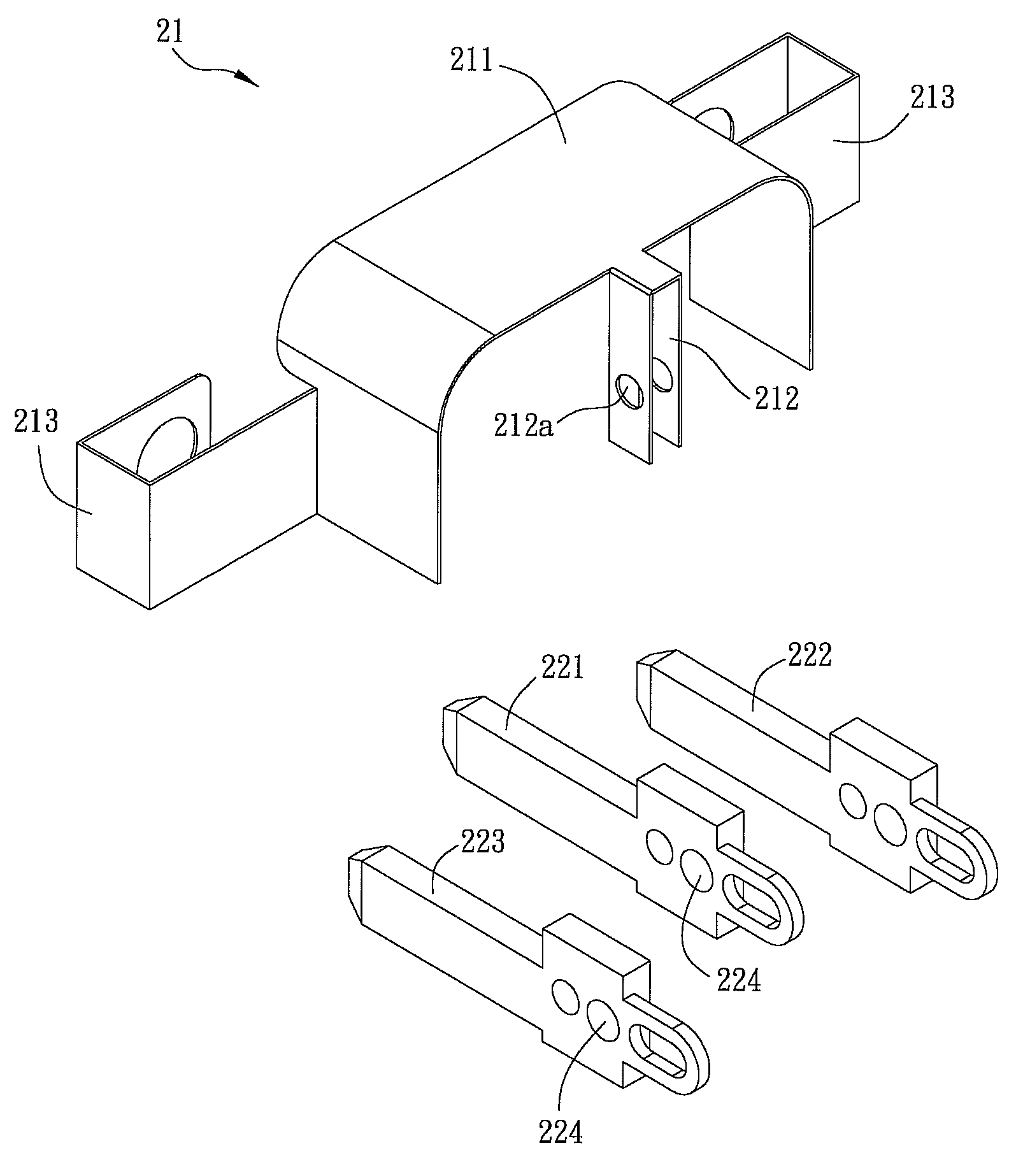
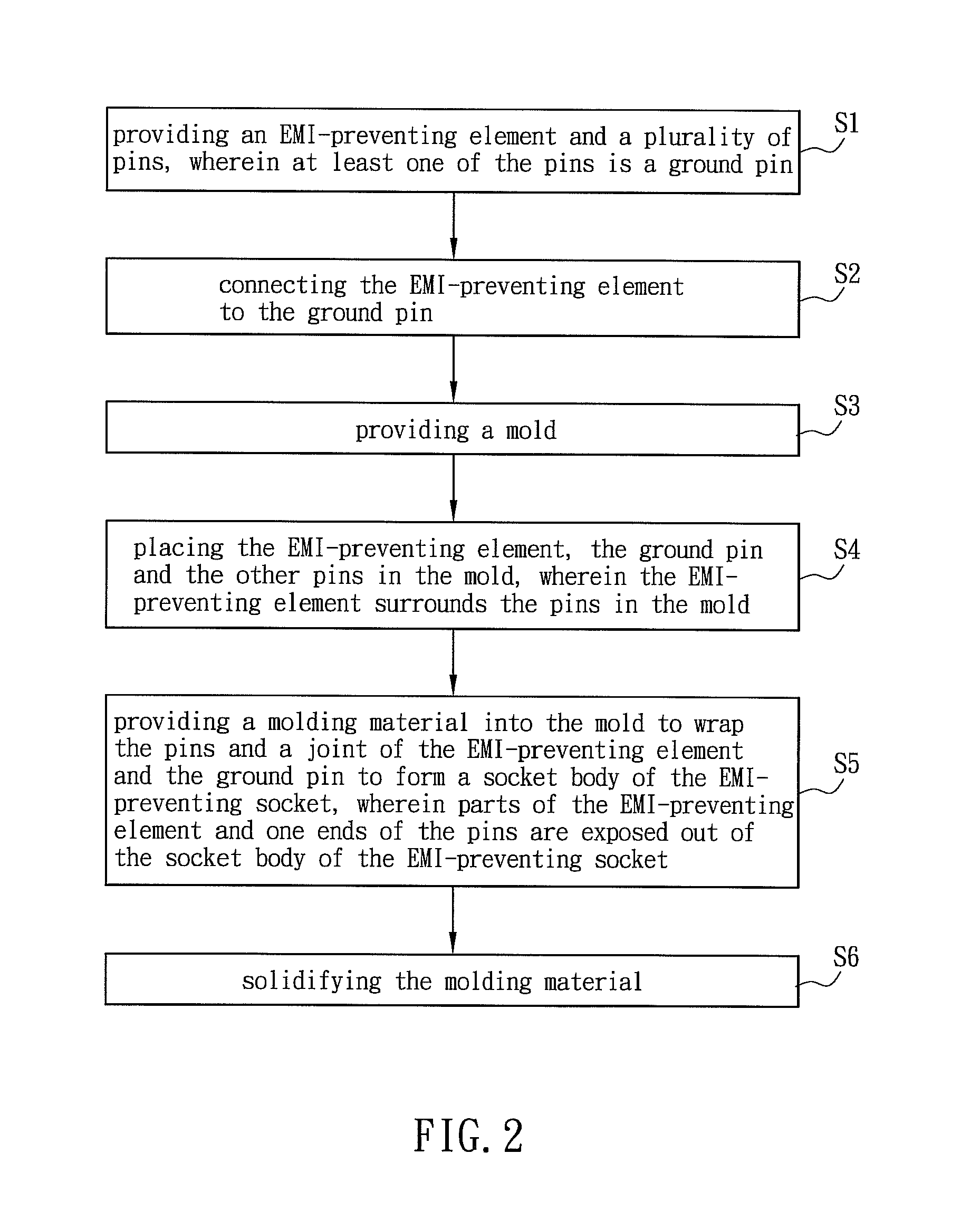
[0022]FIG. 2 is a flow chart of a manufacturing method of an EMI-preventing socket according to a preferred embodiment of the present invention, and FIG. 3 is a schematic diagram showing the EMI-preventing socket during the manufacturing processes. Referring to FIGS. 2 and 3, the EMI-preventing socket of the present embodiment is, for example, a three-hole socket that is suitable for home appliances and factory machines. Of course, the manufacturing method of the invention can also be applied to fabricate other sockets with EMI-preventing function.

[0023]At first, a step S1 is to provide an EMI-preventing element 21 and a plurality of pins 221, 222 and 223. Herein, the pin 221 is a ground pin. The EMI-preventing element 21 is made of electrically conductive material, for example, metal...


PUM

PropertyMeasurementUnit
electrically conductiveaaaaaaaaaa
frequencyaaaaaaaaaa
conductiveaaaaaaaaaa

Abstract

A manufacturing method for an EMI-preventing socket comprises the following steps of providing an EMI-preventing element and a plurality of pins, wherein at least one of the pins is a ground pin; connecting the EMI-preventing element to the ground pin via a direct physical connection; providing a mold; placing the EMI-preventing element, the ground pin and the remaining pins of the plurality of pins in the mold, wherein the EMI-preventing element surrounds the pins in the mold; and providing a molding material into the mold to cover the plurality of pins and to cover a joint of the EMI-preventing element and the ground pin to form a socket body of the EMI-preventing socket. Parts of the EMI-preventing element and one end of each of the plurality of pins is exposed out of the socket body of the EMI-preventing socket.

Description

CROSS REFERENCE TO RELATED APPLICATIONS[0001]This Non-provisional application claims priority under 35 U.S.C. §119(a) on Patent Application No(s). 201110196206.2 filed in People's Republic of China on Jul. 13, 2011, the entire contents of which are hereby incorporated by reference.BACKGROUND OF THE INVENTION[0002]1. Field of Invention[0003]The present invention relates to a manufacturing method of a socket and, in particular, to a manufacturing method of an EMI-preventing socket.[0004]2. Related Art[0005]Electromagnetic interference (EMI) may decrease the performance of devices, apparatuses or systems, or cause harmful electromagnetic results which damage lives or inorganic materials. EMI are usually derived from electromagnetic noises, useless signals, or the changes of the transmitting medium itself. If high-frequency wave energy and signal modulation are used, the radiation may be easily leaked from the transmitting medium. To solve the EMI problem, it is usually to configure the...

Claims


Application Information

Patent Timeline
Patent Type & Authority Patents(United States)
IPC IPC(8): H01R43/24H01R13/6581
CPCH01R43/24H01R13/6581Y10T29/49117Y10T29/49169
Inventor LIU, GANG
Owner DELTA ELECTRONICS (SHANGHAI) CO LTD
Why Eureka
Try Eureka