Liquid crystal display panel and pixel structure

a liquid crystal display panel and pixel structure technology, applied in the field of pixel structure of liquid crystal display panel and pixel structure thereof, can solve the problems of limited viewing angle of lcds, limited viewing angle of existing ffs lcds with pixel structures in single domain, and limited viewing angle of existing ffs lcds. achieve the effect of favorable display quality

Active Publication Date: 2015-04-14
AU OPTRONICS CORP
View PDF19 Cites 4 Cited by
  • Summary
  • Abstract
  • Description
  • Claims
  • Application Information

AI Technical Summary

Benefits of technology

[0008]The present invention provides a pixel structure capable of eliminating color shift in displaying image.
[0025]The color shift of display image in large viewing angle can be effectively eliminated in the pixel structure of the present invention by the stripe electrodes arranged side by side and having gradually varied included angles along the first direction. Thus, the liquid crystal display panel adopting the pixel structure of the present invention can provide favorable display quality.

Problems solved by technology

However, the LCDs are still subject to the limited viewing angles.
The existing FFS LCD with pixel structures in single domain encounters the color shift issue in large viewing angles.
Thus, an acceptable range of viewing angle of the existing FFS LCD is restricted, and the display quality goes inferior.

Method used


Image

  • Liquid crystal display panel and pixel structure
  • Liquid crystal display panel and pixel structure
  • Liquid crystal display panel and pixel structure

Examples


Embodiment Construction

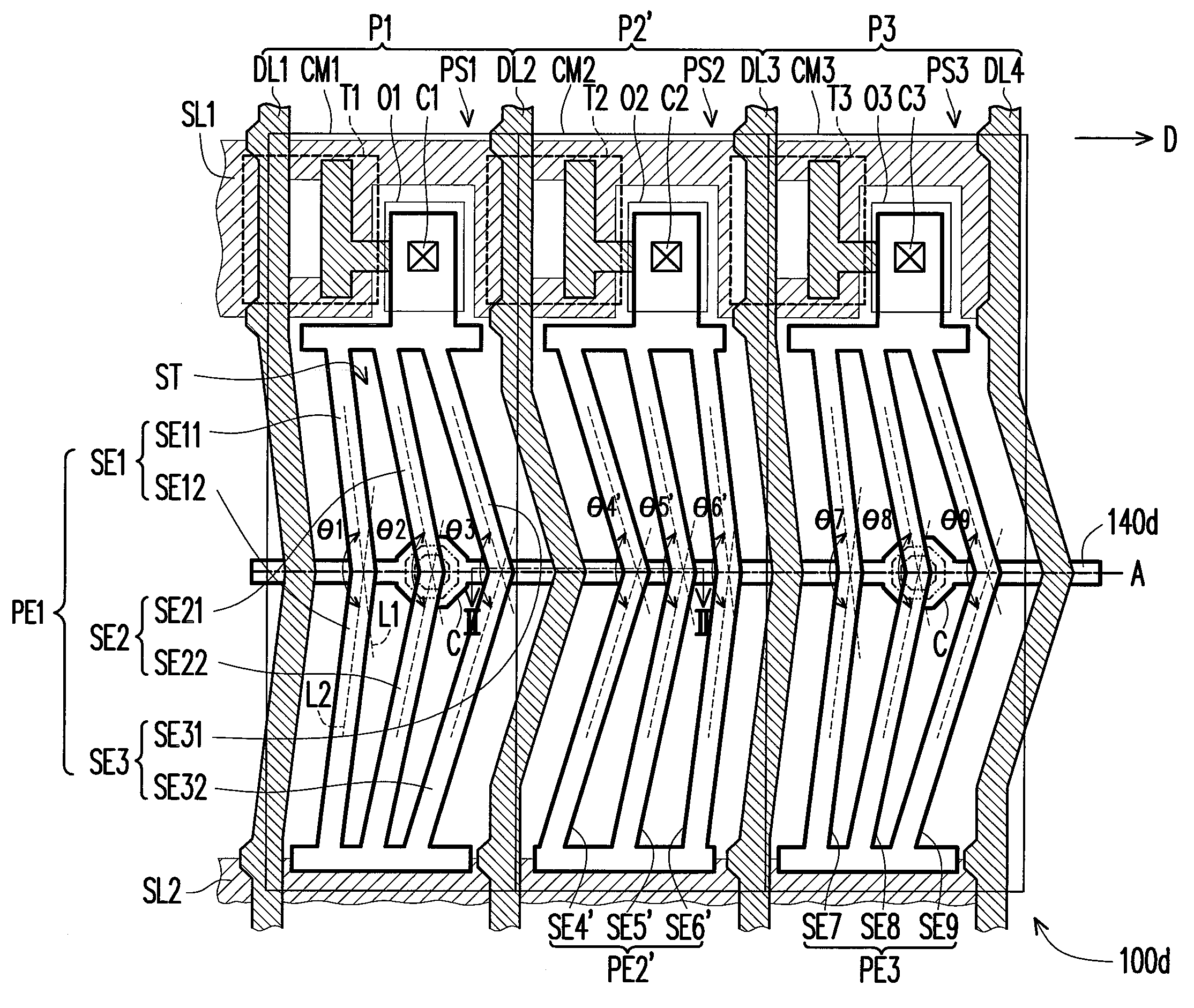
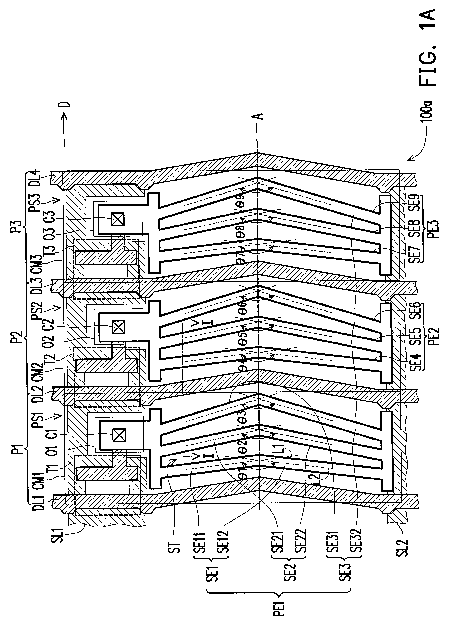
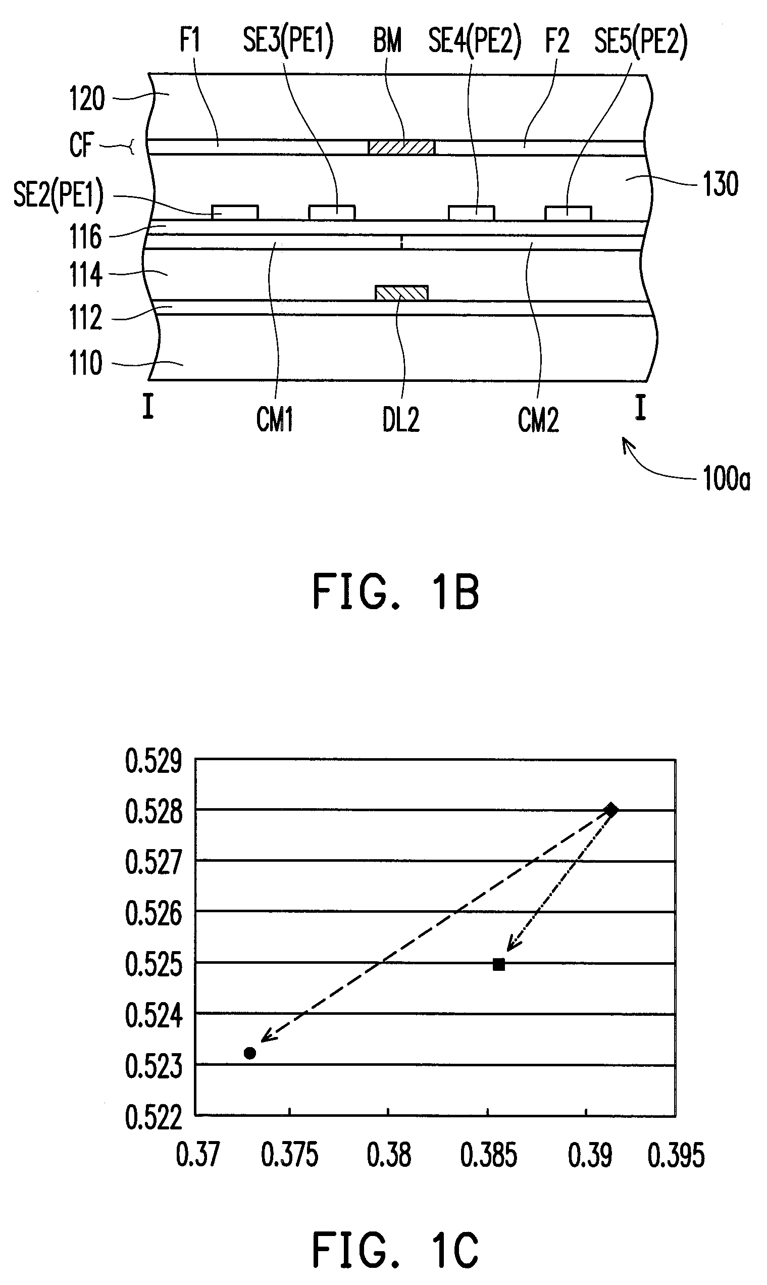
[0036]FIG. 1A is a schematic top view of a liquid crystal display panel according to an embodiment of the present invention. FIG. 1B is a schematic cross-sectional view taken along line I-I in FIG. 1A. For purposes of illustration, some elements shown in FIG. 1B are omitted in FIG. 1A. Referring to FIG. 1A and FIG. 1B, the liquid crystal display panel 100a includes a first substrate 110, a plurality of scan lines (two scan lines SL1 and SL2 are schematically depicted in FIG. 1A), a plurality of data lines (four data lines DL1, DL2, DL3 and DL4 are schematically depicted in FIG. 1A), a plurality of active devices (three active devices T1, T2 and T3 are schematically depicted in FIG. 1A), a plurality of pixel electrodes (three pixel electrodes PE1, PE2 and PE3 are schematically depicted in FIG. 1A), a plurality of common electrodes (three common electrodes CM1, CM2 and CM3 are schematically depicted in FIG. 1A), a second substrate 120, and a liquid crystal layer 130 disposed between t...


PUM

PropertyMeasurementUnit
included anglesaaaaaaaaaa

Abstract

A liquid crystal display panel including a first substrate, scan lines extending along a first direction, data lines, active devices, pixel electrodes, common electrodes, a second substrate and a liquid crystal layer is provided. The pixel electrodes are respectively disposed in sub-pixel regions and coupled to the corresponding active devices. The common electrodes are respectively disposed corresponding to the pixel electrodes. Each common electrode or each pixel electrode includes plural stripe electrodes arranged side by side. Each stripe electrode includes a first section and a second section respectively disposed on two opposite sides of a reference axis, wherein a major axis of the first section forms an included angle with a major axis of the second section. The included angles of the stripe electrodes in each sub-pixel region are gradually varied along the first direction. The liquid crystal layer is disposed between the first substrate and the second substrate.

Description

CROSS-REFERENCE TO RELATED APPLICATION[0001]This application claims the priority benefit of Taiwan application serial no. 101110786, filed on Mar. 28, 2012. The entirety of the above-mentioned patent application is hereby incorporated by reference herein and made a part of this specification.BACKGROUND OF THE INVENTION[0002]1. Field of the Invention[0003]The invention relates to a display panel and pixel structure thereof, and more particularly, to a fringe field switching (FFS) liquid crystal display panel and pixel structure thereof.[0004]2. Description of Related Art[0005]Recently, with continuing maturation of photoelectric technology and semiconductor fabrication, development of flat panel displays is booming. Among the flat panel displays, liquid crystal displays (LCDs) free of harmful radiation and characterized by low operating voltage, light weight, and small volume have gradually replaced conventional cathode ray tube (CRT) displays and have become mainstream display produ...

Claims


Application Information

Patent Timeline
Patent Type & Authority Patents(United States)
IPC IPC(8): G02F1/1343G02F1/1362H01L27/15
CPCG02F1/134363G02F1/1362H01L27/15G02F2001/134372G02F1/134372
Inventor CHANG, WEN-ZONGFAN-JIANG, SHIH-CHYUANCHENG, HSIAO-WEI
Owner AU OPTRONICS CORP
Why Eureka
Try Eureka