Light emitting device package

a technology of light-emitting devices and packaging, which is applied in the direction of semiconductor/solid-state device manufacturing, semiconductor devices, electrical equipment, etc., can solve the problems of shortening of wires, electrically connecting leds and lead frames, etc., and achieve the effect of avoiding potential damage to wires

Inactive Publication Date: 2015-04-21
SAMSUNG ELECTRONICS CO LTD
View PDF7 Cites 10 Cited by
  • Summary
  • Abstract
  • Description
  • Claims
  • Application Information

AI Technical Summary

Benefits of technology

[0012]An aspect of the present invention provides a light emitting device package capable of avoiding potential damage to a wire resulting from a lens pressed in a process of installing a lens in a package main body, and a fabrication method thereof.
[0013]Another aspect of the present invention provides a light emitting device package capable of avoiding damage to a wire by minimizing an occurrence of a phenomenon in which the wire is affected by contraction and expansion of a lens or an encapsulation unit formed through molding.

Problems solved by technology

However, the dome-type lens has a problem in which a wire electrically connecting an LED and a lead frame may be cut by contraction and expansion of the lens.
Thus, when the lens is pressed downwardly during the pick-up process, a wire electrically connecting the LED of the package to a lead frame may be pressed by a lower end portion of the lens reflector and damaged or severed, resulting in a defect such as a short.

Method used


Image

  • Light emitting device package
  • Light emitting device package
  • Light emitting device package

Examples


Embodiment Construction

[0071]Embodiments of the present invention will now be described in detail with reference to the accompanying drawings. The invention may, however, be embodied in many different forms and should not be construed as being limited to the embodiments set forth herein. Rather, these embodiments are provided so that this disclosure will be thorough and complete, and will fully convey the scope of the invention to those skilled in the art. In the drawings, the shapes and dimensions of elements may be exaggerated for clarity, and the same reference numerals will be used throughout to designate the same or like components.

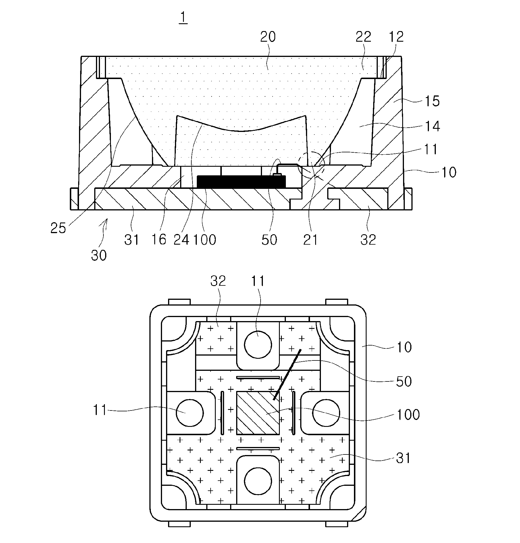
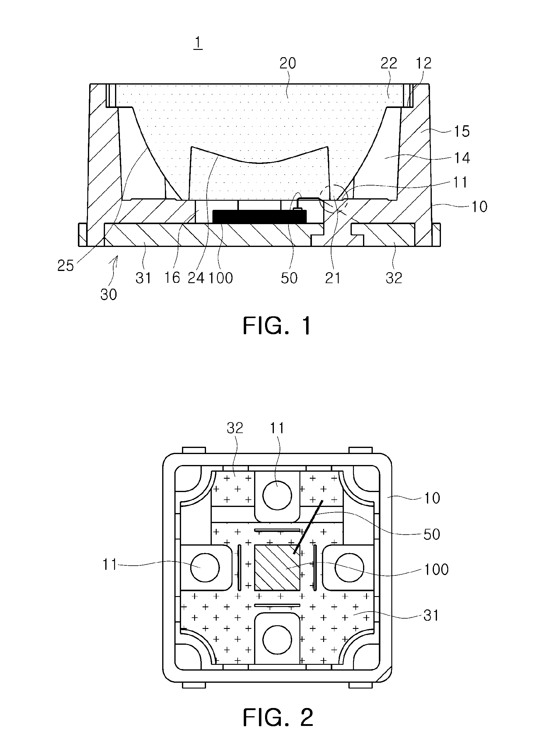
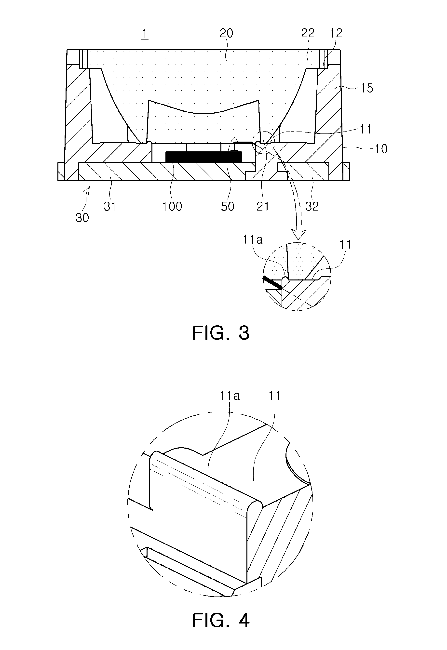
[0072]A light emitting device package according to an embodiment of the present invention will be described with reference to FIGS. 1 and 2. FIG. 1 is a cross-sectional view schematically illustrating a light emitting device package according to an embodiment of the present invention, and FIG. 2 is a plan view of FIG. 1.

[0073]The light emitting device package 1 according t...


PUM


Abstract

A light emitting device package includes: a package main body having a chip mounting region surrounded by side walls; lead frames spaced apart from one another, at least one portion thereof being positioned in the chip mounting region; a light emitting device mounted on the chip mounting region; a wire connecting the lead frame and the light emitting device; a lens disposed on the light emitting device; and a lens support unit formed to be higher than the wire in the chip mounting region and supporting the lens such that the lens does not come into contact with the wire.

Description

CROSS-REFERENCE TO RELATED APPLICATIONS[0001]This application claims the priority of Korean Patent Applications No. 10-2011-0083477 filed on Aug. 22, 2011 and No. 10-2012-0025661 filed on Mar. 13, 2012, in the Korean Intellectual Property Office, the disclosures of which are incorporated herein by references.BACKGROUND OF THE INVENTION[0002]1. Field of the Invention[0003]The present invention relates to a light emitting device package.[0004]2. Description of the Related Art[0005]A light emitting diode (LED), a semiconductor device capable of generating light of various colors according to electron hole recombination occurring in p-type and n-type semiconductor junctions when current is applied thereto, is environmentally-friendly, has a fast response time in the range of a few nano-seconds to thus be effective in displaying a video signal stream, and is available for impulsive driving.[0006]Also, in order to enhance and device responsiveness and luminous intensity distribution, as w...

Claims


Application Information

Patent Timeline
Patent Type & Authority Patents(United States)
IPC IPC(8): H01L33/00H01L27/15H01L29/161H01L25/075H01L33/38H01L33/48H01L33/50H01L33/58
CPCH01L33/58H01L33/486H01L25/0753H01L33/382H01L33/508H01L2224/48091H01L2224/48137H01L2224/49107H01L2224/8592H01L2924/00014H01L2924/181H01L2224/48465H01L2224/73265H01L2924/00012H01L2924/00
Inventor CHOI, SUN
Owner SAMSUNG ELECTRONICS CO LTD
Why Eureka
Try Eureka