
N-path interleaving analog-to-digital converter (ADC) with background calibration

an analog-to-digital converter and background calibration technology, applied in the field of system and method for correcting errors in an npath interleaved analog-to-digital converter, can solve problems such as difficult error detection and impracticality in detection

Active Publication Date: 2015-05-12
IQ ANALOG
View PDF18 Cites 18 Cited by
  • Summary
  • Abstract
  • Description
  • Claims
  • Application Information

AI Technical Summary

Benefits of technology

The patent describes a system and method for calibrating a time-interleaved n-path analog-to-digital converter (ADC). The method uses a first test tone with a known second frequency to determine the phase and amplitude of the test tone. The system then applies corrections to the interleated signal to minimize errors. The corrected signal is then used to determine errors at a different frequency. The system uses a constant sample clock phase difference between paired digital samples and rotates the selection of a digital sample signal to obtain correction information for all the digital samples. The technical effect of this patent is improved accuracy and efficiency in the calibration of time-interleaved n-path ADCs.

Problems solved by technology

As a result, these timing and gain errors produce artifacts that in frequency domain show up as spectral images of the desired signal centered around every multiple of fs / N, where fs is the sampling rate of the composite ADC.
However, without knowing the ADC input signal, error detection is difficult.
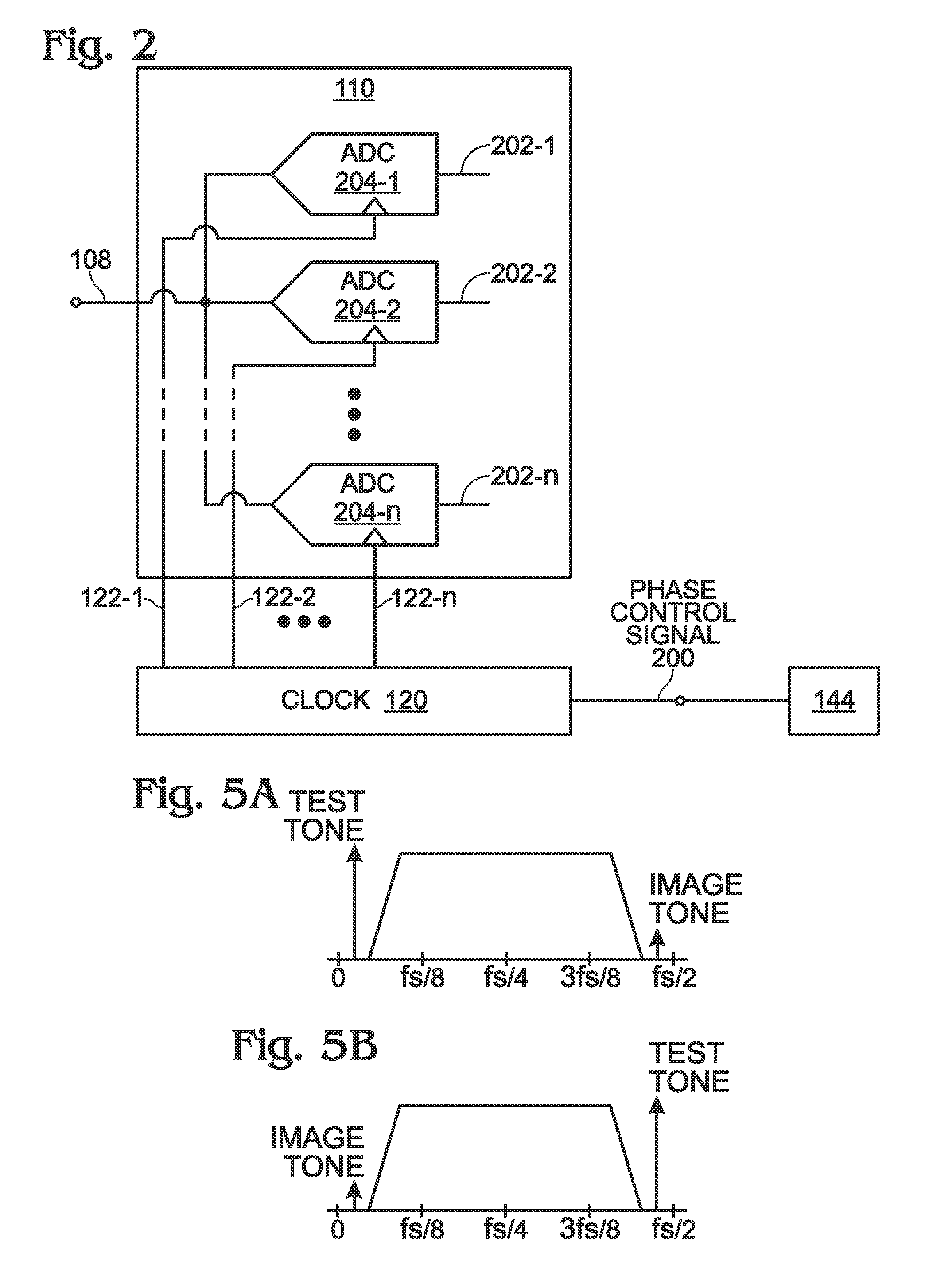
The problem is that only one of the tones is in a frequency region that is free of signal content.
All the other image tones share the same frequencies as the ADC input signal (see FIGS. 6A and 6B) and are impractical to be detected with sufficient accuracy in the background while the ADC input signal is present.

Method used


Image

  • N-path interleaving analog-to-digital converter (ADC) with background calibration
  • N-path interleaving analog-to-digital converter (ADC) with background calibration
  • N-path interleaving analog-to-digital converter (ADC) with background calibration

Examples


Embodiment Construction

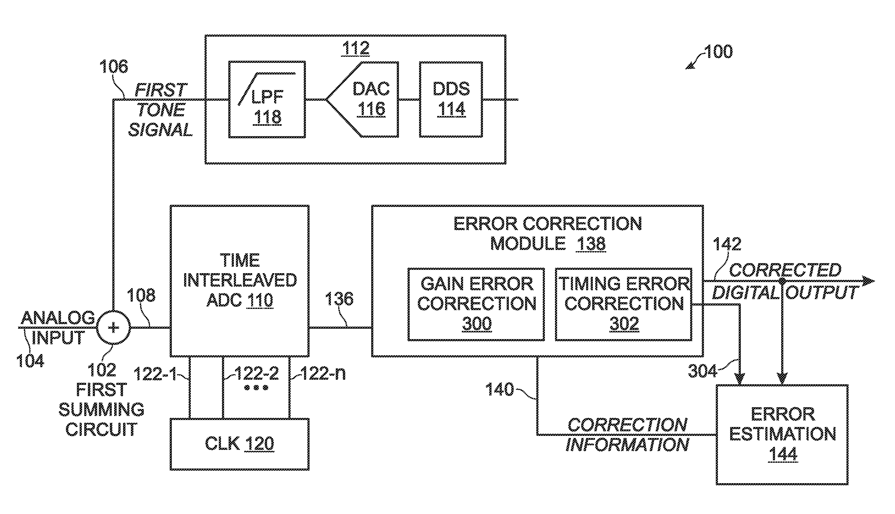
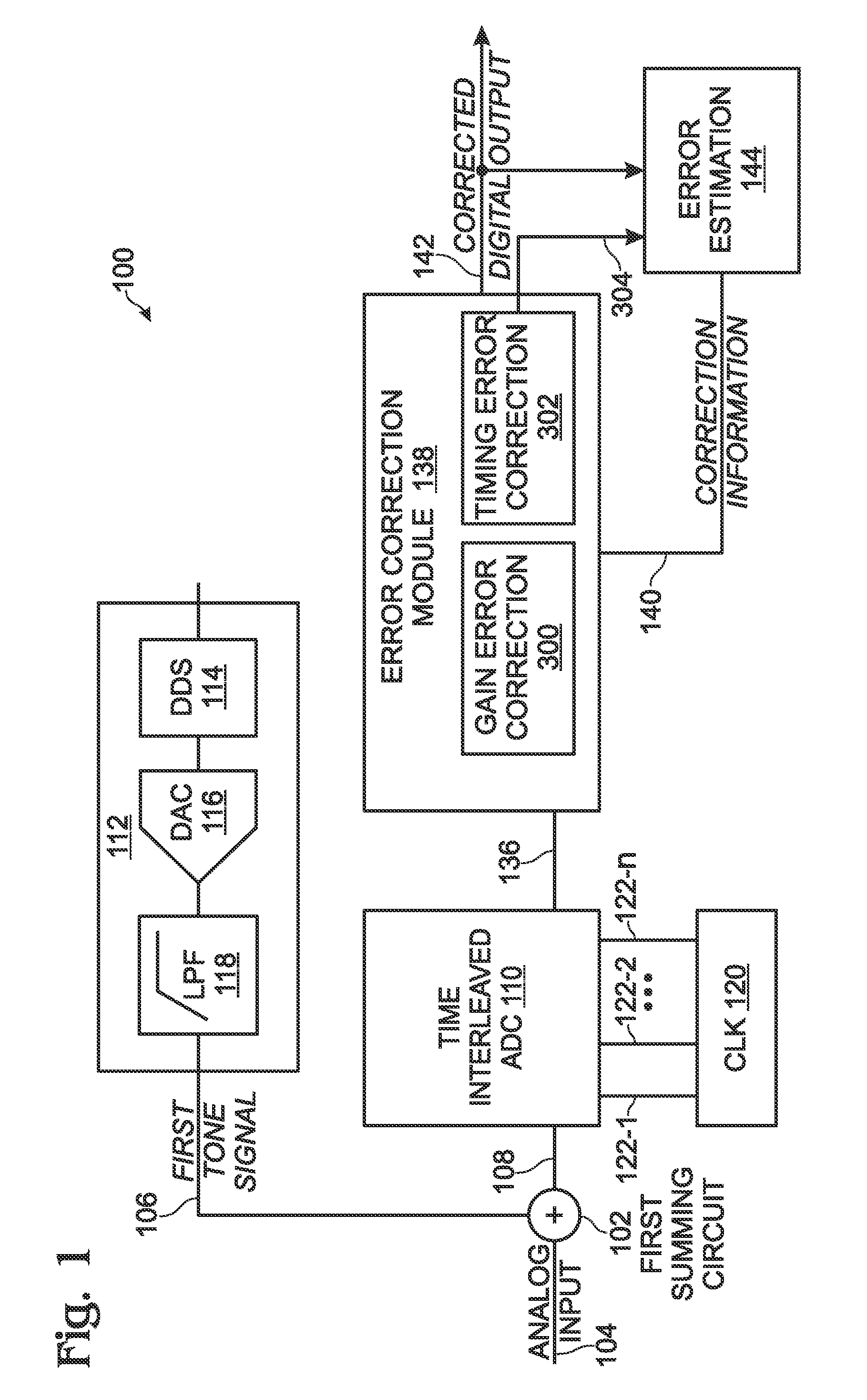
[0026]FIG. 1 is a schematic block diagram depicting a system performing background corrections for an n-path interleaving analog-to-digital converter (ADC). The system 100 comprises a first summing circuit 102 having an input on line 104 to accept an analog input signal s1(t) with a first frequency f1 and a bandwidth (BW). The summing circuit 102 has an input on line 106 to accept a first tone signal s2(t) having a predetermined second frequency f2 outside BW. The first summing circuit 102 has an output on line 108 to supply a combination signal to time interleaved ADC 110. The first tone signal is supplied by signal or pilot tone generator 112. In one aspect, the signal generator 112 comprises a direct digital synthesizer (DDS) 114, digital-to-analog converter (DAC) 116, and lowpass filter 118. However, the system is not limited to any particular means of generating the first tone signal.

[0027]Clock 120 has a clock frequency fs, with outputs on lines 122-1 through 122-n to respecti...


PUM


Abstract

A system and method are provided of performing background corrections for an interleaving analog-to-digital converter (ADC). An analog input signal s1(t) is accepted having a first frequency f1 and a bandwidth (BW). A clock at frequency fs creates n sample clocks with evenly spaced phases, each having a sample clock frequency of fs / 2. A first tone signal s2(t) is generated at second frequency f2, outside BW. The analog input signal and the first tone signal are combined, creating a combination signal, which is sampled using the sample clocks, creating n digital sample signals per clock period 1 / fs. The n digital sample signals are interleaved, creating an interleaved signal. Corrections are applied that minimize errors in the interleaved signal, to obtain a corrected digital output. Errors are determined at an alias frequency f3, associated with the second frequency f2, to obtain correction information for a rotating pair of digital sample signals.

Description

RELATED APPLICATIONS[0001]This application, is a Continuation-in-part of an application entitled, INTERLEAVING ANALOG-TO-DIGITAL CONVERTER (ADC) WITH BACKGROUND CALIBRATION, invented by Mikko Waltari et al., Ser. No. 14 / 511,206, filed Oct. 10, 2014, now U.S. Pat. No. 8,917,125, issued on Dec. 23, 2014;[0002]which is a Continuation-in-part of an application entitled, SYSTEM AND METHOD FOR FREQUENCY MULTIPLIER JITTER CORRECTION, invented by Mikko Waltari et al., Ser. No. 14 / 081,568, filed Nov. 15, 2013, now U.S. Pat. No. 8,878,577, issued on Nov. 4, 2014;[0003]which is a Continuation-in-Part of an application entitled, TIME-INTERLEAVED ANALOG-TO-DIGITAL CONVERTER FOR SIGNALS IN ANY NYQUIST ZONE, invented by Mikko Waltari, Ser. No. 13 / 603,495, filed Sep. 5, 2012, issued as U.S. Pat. No. 8,654,000 on Feb. 18, 2014. All these application are incorporated herein by reference.BACKGROUND OF THE INVENTION[0004]1. Field of the Invention[0005]This invention, generally relates to analog-to-digi...

Claims


Application Information

Patent Timeline
Patent Type & Authority Patents(United States)
IPC IPC(8): H03M1/06H03M1/12
CPCH03M1/0617H03M1/1245H03L7/18H03M1/0626H03M1/124H03M1/0836H03M1/1215
Inventor WALTARI, MIKKO
Owner IQ ANALOG
Learn More