Controlled switch for opening or closing on demand a section of an electrical circuit of a power stage

a technology of power stage and control switch, which is applied in the direction of pulse technique, dc-dc conversion, power conversion system, etc., can solve the problems of high voltage vsub>ds of mos transistors that are costly and/or unsuitable for production and application via reliable, and achieve reliable and cost-efficient industrial processes.

Active Publication Date: 2015-06-02
GUANGDONG OPPO MOBILE TELECOMM CORP LTD
View PDF5 Cites 0 Cited by
  • Summary
  • Abstract
  • Description
  • Claims
  • Application Information

AI Technical Summary

Benefits of technology

[0004]A need therefore exists for a controlled switch which opens or closes a section of an electrical circuit, particularly a power stage, in which a current having a voltage on the order of 6V can flow, wherein said switch can be manufactured and integrated during mass production using reliable and cost-efficient industrial processes.
[0017]Thus when the second transistor is non-conducting, the current between the first node and the second node is zero. As the gate of the first transistor is maintained at the first electrical potential, the intermediate connecting point between the first transistor and the second transistor is also polarized to the first potential. However, the value of the first potential is between that of the potential at the first node and that of the potential at the second node. Thus the maximum voltage between the intermediate connecting point and the second connecting point must be less than the voltage between the first node and the second node. Therefore the first and second transistor must each support a voltage, between their source and their drain, that is less than what has to be supported by a single transistor used as a switch. By reducing the maximum voltage supported by the first and the second transistor, it becomes possible to use manufacturing processes for the switch which are industrially efficient and less costly. It also becomes possible for the switch to be integrated.
[0035]The first transistor and second transistor of the first switch can be effectively and easily controlled using the second and third potential. It is then unnecessary to generate intermediate potentials, which simplifies the driving circuit and reduces the design and production costs, the difference between the first potential and the second potential being greater than or equal to the threshold voltage of the first and second transistors, and the opposite of the value of the third potential being greater than the threshold voltage of the first and second transistors. The device may also be efficiently implemented by using industrially efficient and less costly production methods, as it comprises switches according to the first aspect.
[0041]The control of the first transistor and the second transistor of the first switch can be efficiently and easily implemented using the second and the reference potential, or ground, of the circuit. It is therefore unnecessary to generate intermediate potentials, which simplifies the driving circuit and reduces the design and production costs. The device can also be efficiently implemented using industrially effective and less costly manufacturing processes, as it comprises switches according to the second aspect.
[0051]Indeed, when it is open, the second switch suppresses leakage currents, particularly due to the back-to-back assembly of the body diodes of the third and fourth transistor and due to the change in potential of the fourth control input according to the polarity of the third terminal.

Problems solved by technology

In the case of a power stage configured to provide a positive potential VPOS of about 1.8 V and the negative potential VNEG of about −1.8 V, from the potential VBAT of 4.8 V supplied by a battery, the voltage VDS may reach 6.6 V. However, the MOS transistors able to support such a high voltage VDS are costly and / or unsuitable for production and application via reliable and cost-efficient industrial processes, particularly for the mass production of electrical circuits such as those used in the manufacture of mobile telephones.

Method used


Image

  • Controlled switch for opening or closing on demand a section of an electrical circuit of a power stage
  • Controlled switch for opening or closing on demand a section of an electrical circuit of a power stage
  • Controlled switch for opening or closing on demand a section of an electrical circuit of a power stage

Examples


Embodiment Construction

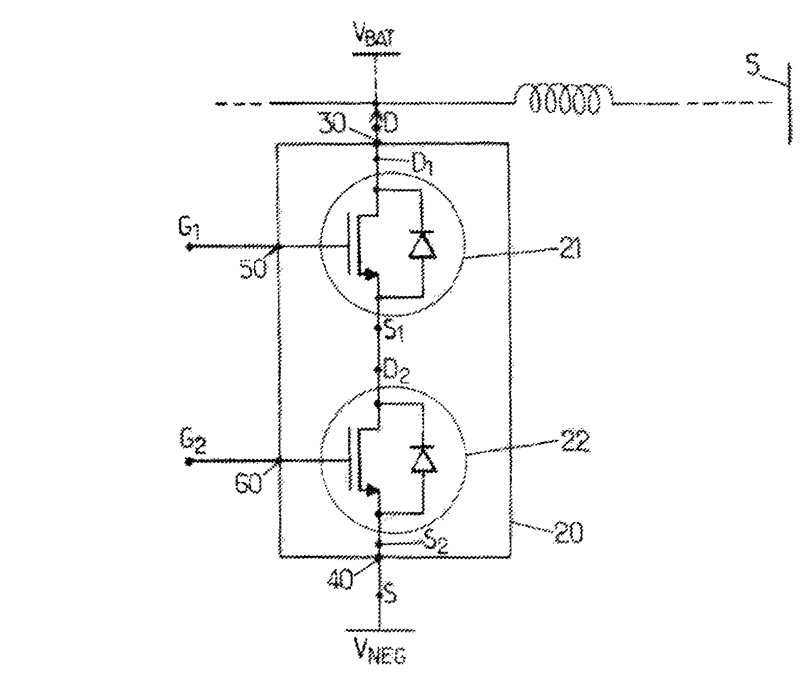
[0069]In this description, when it refers to a voltage at a node of a circuit, this is understood to mean the difference between the potential at said node and a reference potential common to the entire circuit. The reference potential is also commonly referred to as the ground, and has a value that is generally equal to 0V.

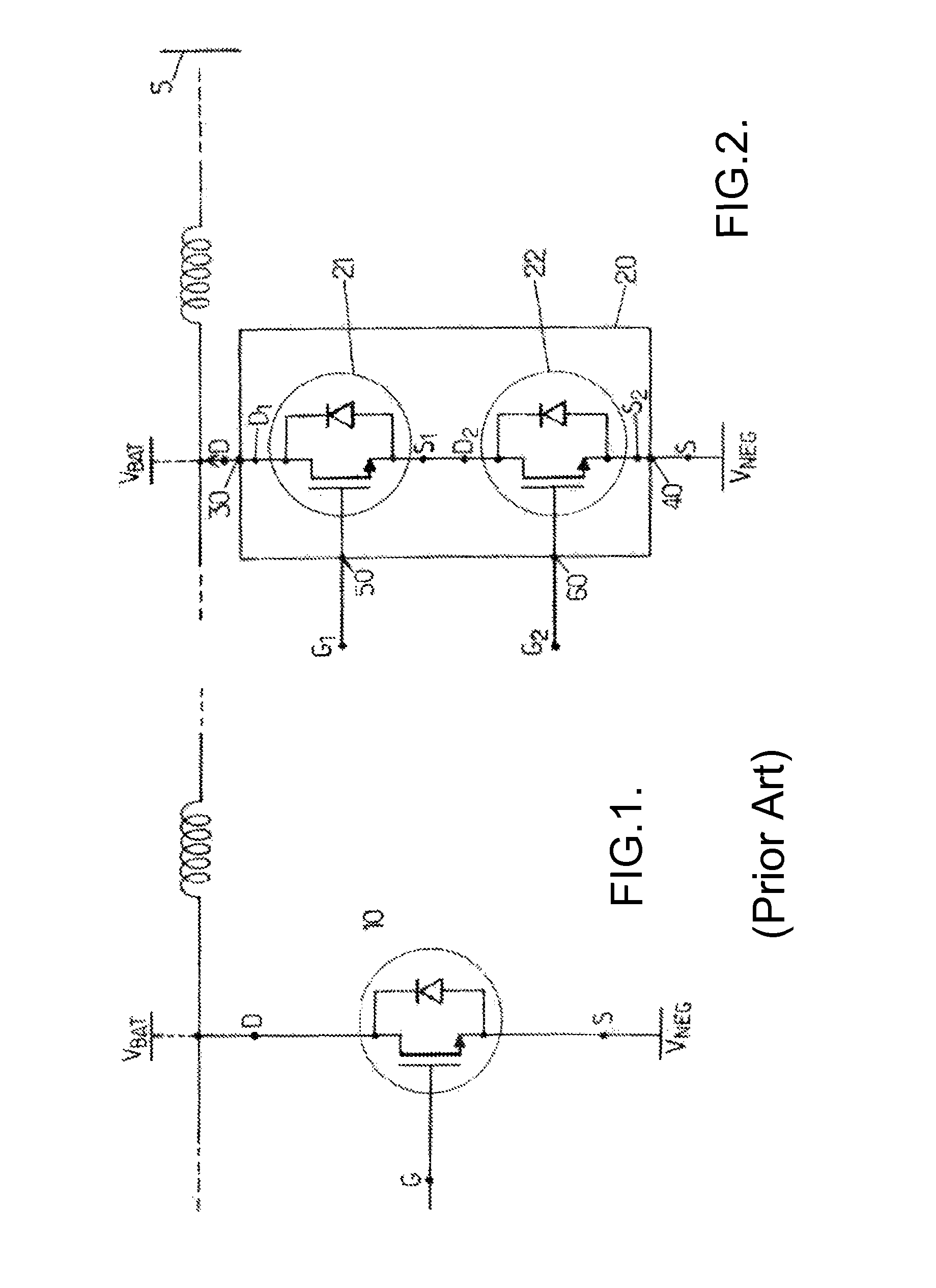
[0070]One embodiment of a controlled switch 20, included in a section of an electrical circuit 5 of a power stage, is represented in FIG. 2. The switch 20 comprises a first coupling node 30 and a second coupling node 40. The switch 20 also comprises at least a first control input 50 and a second control input 60. The switch 20 is adapted to open or close an electrical circuit between the first coupling node 30 and the second coupling node 40, as a function of the control voltages received on the first input 50 and the second input 60. In the example in FIG. 2, the first coupling point 30 is coupled to a node D of the circuit 5, and the second coupling point 40 to...


PUM


Abstract

The invention proposes a voltage regulating device having a switch in an electrical circuit between a first node (30, 140) and a second node (40, 130), comprising a first field effect transistor (21, 110) and a second field effect transistor (22, 120) connected in cascade. The switch is controlled by: —setting the gate (G1,G3) of the first transistor to a first electrical potential, and, —to close the switch, setting the gate (G2, G4) of the second transistor to the first potential, or —to open the switch, setting the gate of the second transistor to the electrical potential of the second node, with the difference between the first potential and the second potential then being adapted to allow opening the first transistor and the second transistor. The switch can be used in a switched-mode power supply.

Description

TECHNICAL DOMAIN[0001]This invention relates in general to controlled switches used in integrated circuits. It more particularly concerns devices for opening or closing on demand a section of an electrical circuit of a power stage, in a switched-mode power supply.TECHNOLOGICAL BACKGROUND[0002]In power stages, a switch controlled by a control signal is typically implemented by a metal-oxide-semiconductor transistor, commonly referred to using the acronym “MOS”. A MOS transistor is driven by a control voltage. FIG. 1 shows a section of a power stage of a switched-mode power supply comprising a switch 10 controlled by control voltage VG. The controlled switch 10 is a MOS transistor comprising a gate coupled to a node G, a drain coupled to a node D which is brought to a potential VBAT, and a source coupled to a node S which is brought to a potential VNEG. The control voltage VG is applied to the node G. Depending on the value of the control voltage VG, the voltage VDS between the source...

Claims


Application Information

Patent Timeline
Patent Type & Authority Patents(United States)
IPC IPC(8): G05F1/00H02M1/00H02M1/08H02M3/158H03K17/10H03K17/687
CPCH02M1/08H03K17/102H03K17/6874H02M3/1582H02M2001/009H02M1/009
Inventor BRANCA, XAVIERCHESNEAU, DAVID
Owner GUANGDONG OPPO MOBILE TELECOMM CORP LTD
Why Eureka
Try Eureka