Techniques for quantifying fin-thickness variation in FINFET technology
a technology of finfet and fin thickness, applied in the direction of semiconductor/solid-state device testing/measurement, electric/magnetic measurement arrangement, instruments, etc., can solve the problems of destroying wafers and consuming a lot of tim
- Summary
- Abstract
- Description
- Claims
- Application Information
AI Technical Summary
Benefits of technology
Problems solved by technology
Method used
Image

Examples
Embodiment Construction
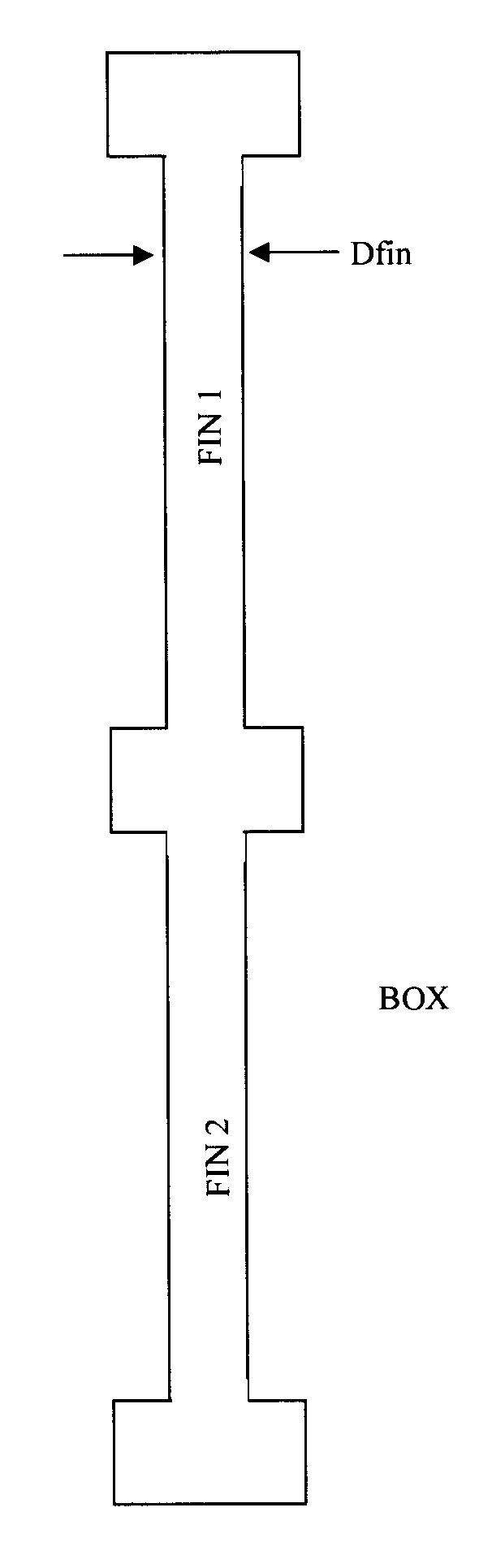
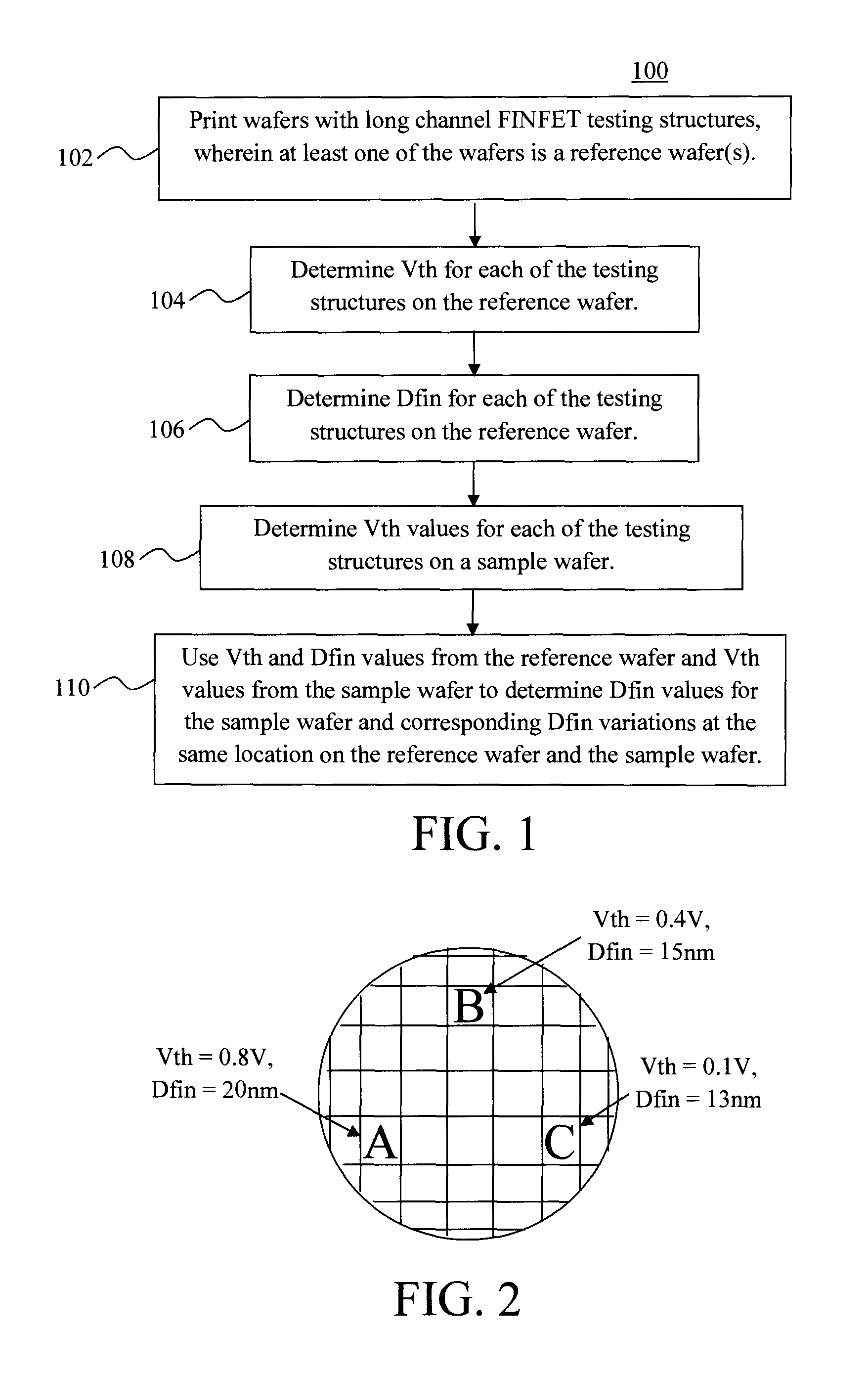
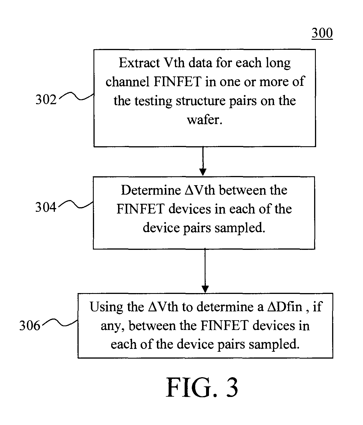
[0021]Provided herein are techniques for systematically and efficiently quantifying FIN field effect transistor (FINFET) fin thickness (Dfin) variations (ΔDfin) across a chip without causing damage to the wafer. The present techniques make use of the discovery that the difference in threshold voltage (Vth)−ΔVth—between pairs of long channel FINFET devices is proportional to the difference in fin thickness (Dfin)−ΔDfin—between these devices (also referred to herein as fin thickness variation). This relationship can then be used to quantify long channel FINFET ΔDfin for any sample wafer based on Vth values for at least two long channel FINFET devices on the wafer. The present techniques can be implemented to analyze systematic / global processing fin thickness variations (ΔDfin), as well as local / random fin thickness variations (ΔDfin) that occur on the wafer. Systematic / global variations are variations that occur on a wafer-by-wafer basis, and are typically caused by variations in the ...
PUM
 Abstract
Description
Claims
Application Information
 - Generate Ideas
- Intellectual Property
- Life Sciences
- Materials
- Tech Scout
- Unparalleled Data Quality
- Higher Quality Content
- 60% Fewer Hallucinations
Browse by: Latest US Patents, China's latest patents, Technical Efficacy Thesaurus, Application Domain, Technology Topic, Popular Technical Reports.
© 2025 PatSnap. All rights reserved.Legal|Privacy policy|Modern Slavery Act Transparency Statement|Sitemap|About US| Contact US: help@patsnap.com