
Negative pixel compensation

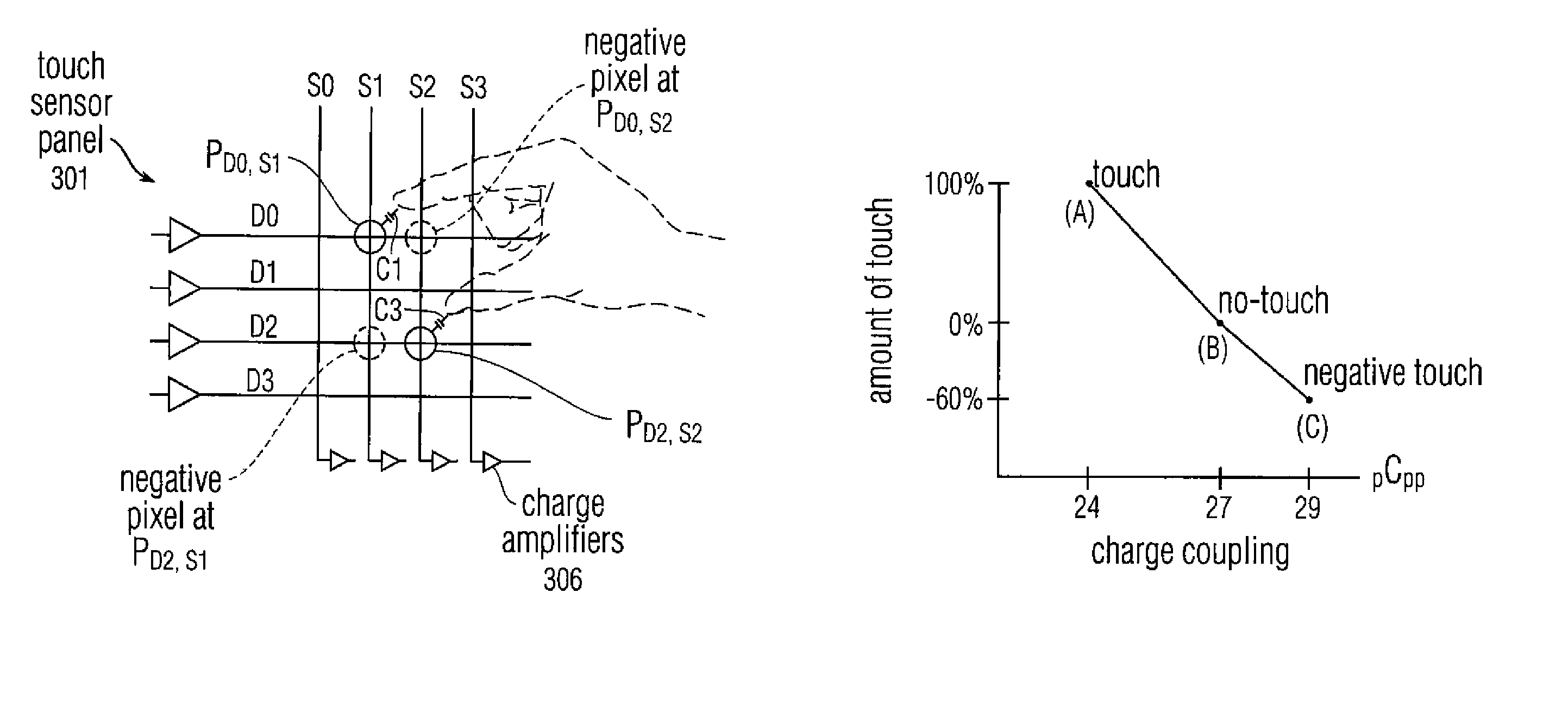
a technology of negative pixel and compensation, applied in the field of multi-touch sensor panels, can solve the problems of false, erroneous or otherwise distorted readings of certain pixels, and achieve the effect of reducing capacitance, minimizing negative pixels, and negative pixel effects

Active Publication Date: 2015-07-07
APPLE INC
View PDF21 Cites 1 Cited by
  • Summary
  • Abstract
  • Description
  • Claims
  • Application Information

AI Technical Summary

Benefits of technology

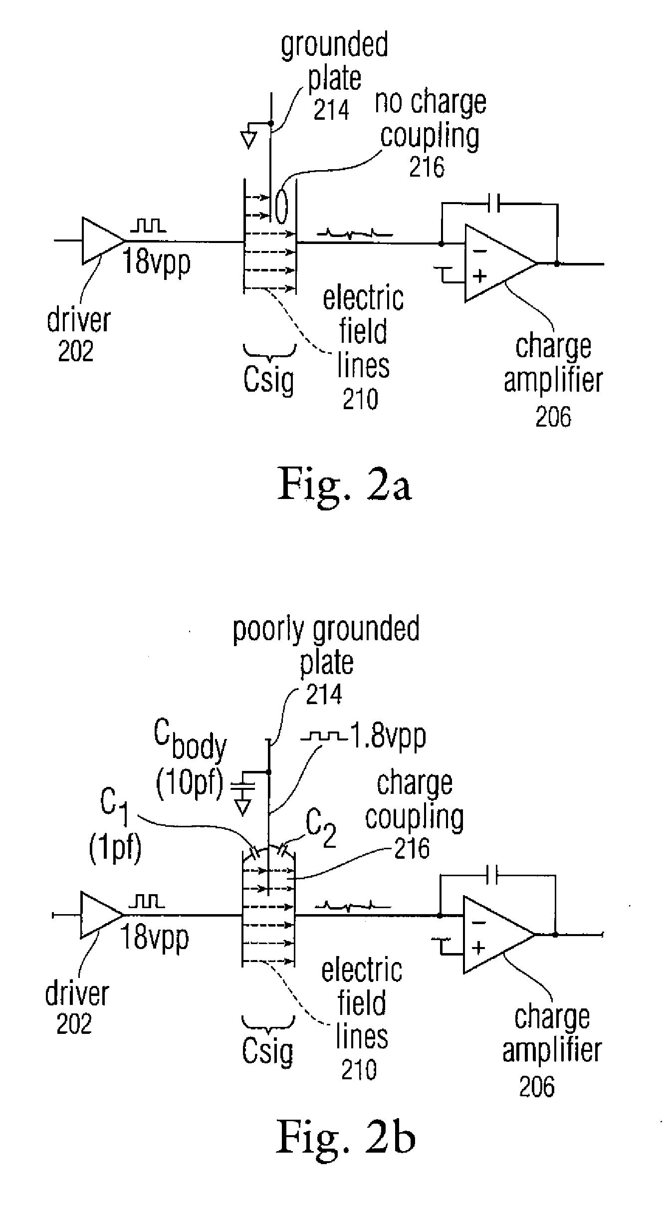
The patent text discusses a method to minimize negative pixels in mechanical devices. It suggests using a thicker cover material or a cover material with a lower dielectric constant. This can reduce the negative pixel effect by making the charge coupling process pass through the cover material twice, which is like two capacitors in series. Alternatively, narrower lines can be used to reduce the number of electric field lines and thus less charge coupling. Overall, this method helps improve the quality of the image captured by the device.

Problems solved by technology

In multi-touch sensor panels, certain pixels can generate false, erroneous or otherwise distorted readings when two or more simultaneous touch events are generated by the same poorly grounded object.

Method used


Image

  • Negative pixel compensation
  • Negative pixel compensation
  • Negative pixel compensation

Examples


Embodiment Construction

[0026]In the following description of preferred embodiments, reference is made to the accompanying drawings which form a part hereof, and in which it is shown by way of illustration specific embodiments in which the invention can be practiced. It is to be understood that other embodiments can be used and structural changes can be made without departing from the scope of the embodiments of this invention.

[0027]This relates to the compensation of pixels that generate false, erroneous or otherwise distorted readings when two or more simultaneous touch events are generated by the same poorly grounded object on a touch sensor panel. For purposes of this disclosure, “poorly grounded” may be used interchangeably with “ungrounded” or “floating” and includes poor grounding conditions that exist when the object (e.g. the user) is not making a low resistance electrical connection to the ground of the device employing the touch sensor panel. To compensate for these distorted readings, which can...


PUM


Abstract

Compensation of pixels that generate erroneous readings (so-called “negative pixels”), produced when multiple touch events are generated by the same poorly grounded object on a touch sensor panel is disclosed. To minimize negative pixels, a thicker cover material and / or a lower dielectric constant can be used. Alternatively, narrower drive and sense lines can be employed. To compensate for negative pixels, a predicted negative pixel value can be computed as an indicator of pixels that are likely to be distorted. The negative pixel value for any particular pixel can be computing by summing up the touch output values for pixels in the drive line of that pixel, summing up the touch output values for pixels in the sense line of that pixel, and then multiplying these two sums. The predicted negative pixel value is added to the measured touch output value for the pixel to compensate for artificially negative readings.

Description

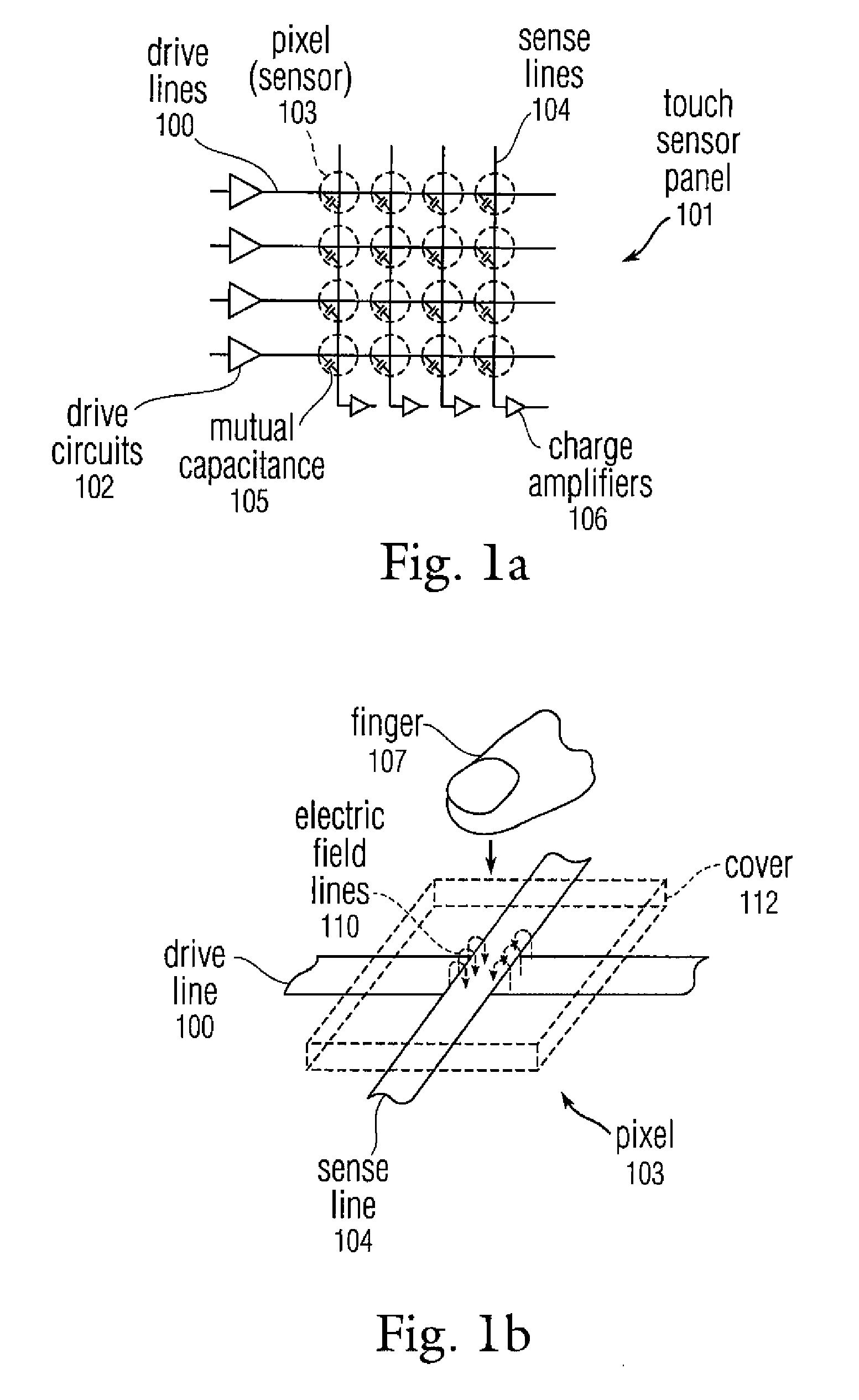
FIELD OF THE INVENTION[0001]This relates to multi-touch sensor panels that utilize an array of capacitive sensors (pixels) to detect and localize touch events, and more particularly, to the compensation of pixels having distorted readings when two or more simultaneous touch events are generated by the same poorly grounded object.BACKGROUND OF THE INVENTION[0002]Many types of input devices are presently available for performing operations in a computing system, such as buttons or keys, mice, trackballs, touch sensor panels, joysticks, touch screens and the like. Touch screens, in particular, are becoming increasingly popular because of their ease and versatility of operation as well as their declining price. Touch screens can include a touch sensor panel, which can be a clear panel with a touch-sensitive surface, and a display device that can be positioned behind the panel so that the touch-sensitive surface can substantially cover the viewable area of the display device. Touch scree...

Claims


Application Information

Patent Timeline
Patent Type & Authority Patents(United States)
IPC IPC(8): G06F3/041G06F3/044
CPCG06F3/044G06F3/0418G06F3/04186G06F3/0446
Inventor WESTERMAN, WAYNE CARLHOTELLING, STEVE PORTER
Owner APPLE INC
Learn More