Light emitting diode circuitry, method for driving light emitting diode circuitry and display

a technology of light-emitting diodes and circuits, applied in the direction of electroluminescent light sources, static indicating devices, instruments, etc., can solve the problems of deteriorating the image retention effect of displays, the service life of oled displays is still relatively short,

Active Publication Date: 2015-07-14
AU OPTRONICS CORP
View PDF6 Cites 9 Cited by
  • Summary
  • Abstract
  • Description
  • Claims
  • Application Information

AI Technical Summary

Benefits of technology

[0028]In view of above, through utilizing the devices and methods in aforementioned embodiments, the image retention effect of displays can be reduced and the service life of displays can be greatly extended. Besides, the situation that the brightness of light emitting diodes is affected by the threshold voltage of transistor elements can be avoided.

Problems solved by technology

However, comparing with liquid crystal displays and LED displays, the service life of OLED displays are still relatively short.
However, under this configuration, the voltage level of the cathode of the light emitting diode D1 will gradually become higher, causing the current following from the first power source VDD through the light emitting diode D1 become smaller, thus deteriorating the image retention effect of displays.

Method used


Image

  • Light emitting diode circuitry, method for driving light emitting diode circuitry and display
  • Light emitting diode circuitry, method for driving light emitting diode circuitry and display
  • Light emitting diode circuitry, method for driving light emitting diode circuitry and display

Examples


first embodiment

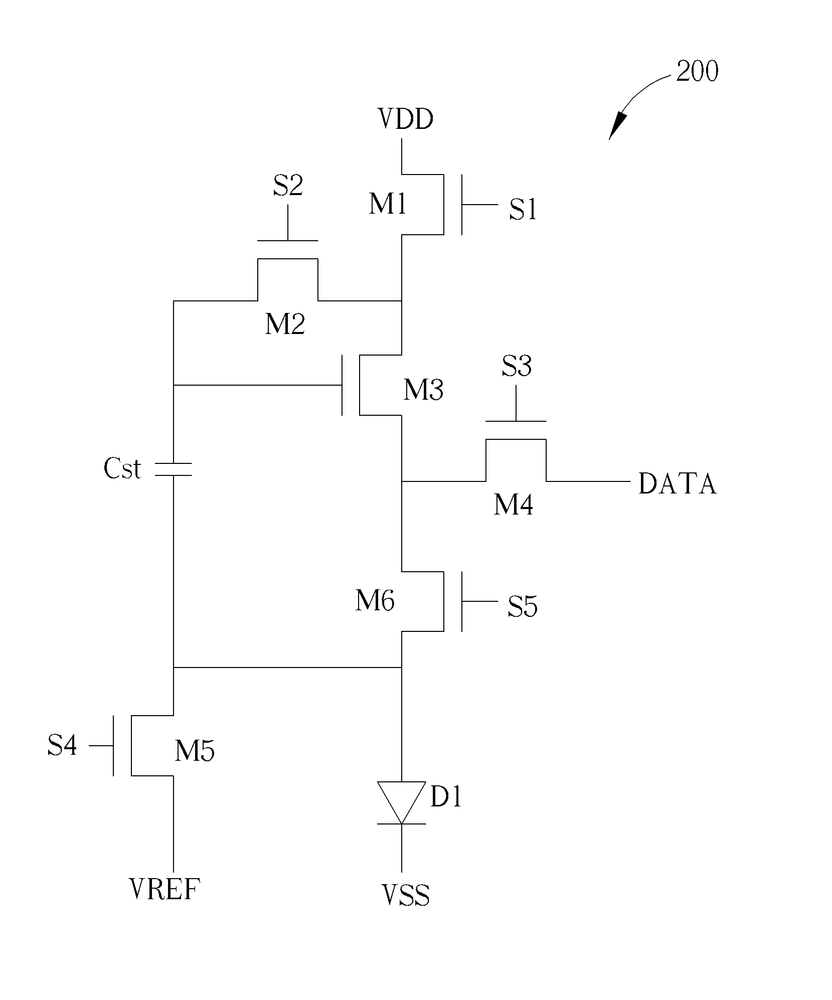
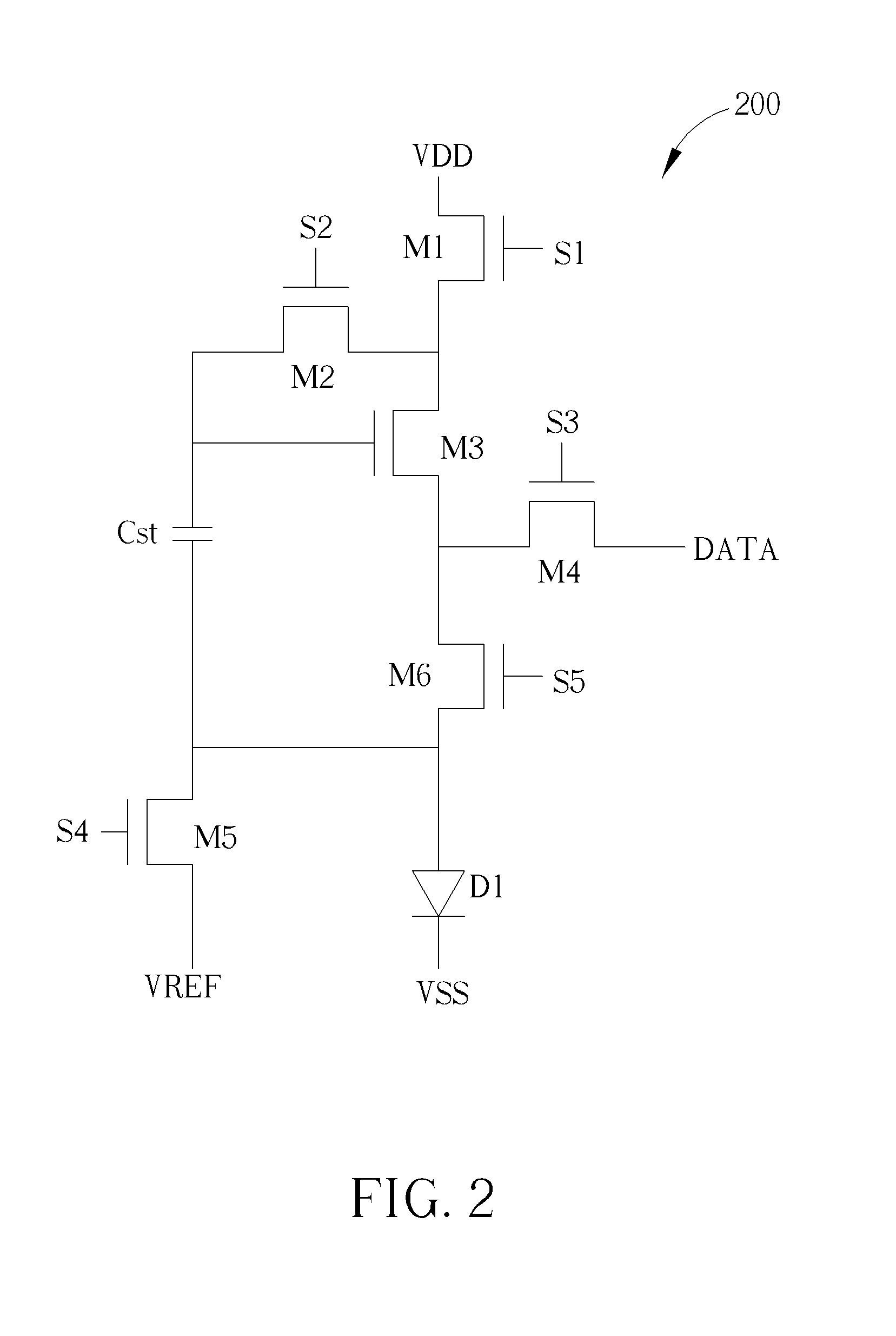
[0022]During the write stage, after writing the data signal DATA into the storage capacitor Cst, the voltage level stored in the storage capacitor Cst equals to (VDATA+Vth−VVREF). VDATA denotes the voltage level of the data signal DATA, Vth denotes the threshold voltage of a transistor, and VVREF denotes the voltage level of the reference voltage source VREF. Therefore, during the emitting stage, the voltage level stored in the storage capacitor Cst will definitely turn on the third transistor M3, so that the third transistor M3 can be operated under the saturation region, at this time, the current flowing from the third transistor M3 to the LED D1 is proportional to (Vgs-Vth)2. Vgs denotes the gate-to-source voltage of a transistor. The gate-to-source voltage of the third transistor M3 equals to the difference between the voltage level of the second end of the third transistor M3 and the difference between the voltage level of the control end of the third transistor M3. Therefore, ...

third embodiment

[0025]Please refer to FIG. 5 with FIG. 2 and FIG. 4. FIG. 5 shows a display 500 according to the present invention. The display 500 includes a power supply 520, a reference voltage source generating unit 530, a scan driver 540, a data driver 560, a timing controller 580 and a plurality of light emitting diode circuitries 200. The power supply 520 is used for providing a first power source VDD and a second power source VSS (referring to FIG. 2), and the first power source VDD and the second power source VSS can be delivered by a first power trace and a second power trace (referring to the first power trace LV1 and the second power trace LV2 in FIG. 4). The reference voltage source generating unit 530 is used for providing a reference voltage source VREF, and the reference voltage source VREF can be delivered by a reference voltage source trace (referring to the reference voltage source trace LV3 in FIG. 4). The scan driver 540 is used for providing a first control signal S1, a second...


PUM


Abstract

A light emitting diode circuitry includes a first transistor, a second transistor, a third transistor, a fourth transistor, a storage capacitor, a fifth transistor, a sixth transistor and light emitting diodes. The first transistor is used for receiving a first control signal. The second transistor is used for receiving a second control signal. The third transistor is electrically coupled to the second transistor and the first transistor. The fourth transistor is used for receiving a data signal and a third control signal. The storage capacitor is electrically coupled to the second transistor. The fifth transistor is used for receiving a fourth control signal. The sixth transistor is used for receiving a fifth control signal. The light emitting diodes are coupled to the sixth transistor and a power source.

Description

BACKGROUND[0001]1. Technical Field[0002]The present invention relates to a light emitting diode circuitry, especially to a light emitting diode circuitry applied to light emitting diode displays.[0003]2. Description of the Prior Art[0004]Liquid crystal displays (LCDs) and light emitting diode (LED) displays are widely used nowadays. Because liquid crystal displays and LED displays have slim shapes, low power dissipation and low radiation, liquid crystal displays and LED displays gradually replace traditional CRT (cathode ray tube) monitors and are widely used in mobile electronic devices such as notebooks and PDAs (personal digital assistants).[0005]Compared to LCDs, organic light emitting diode (OLED) displays are capable of self-emitting light and have wider viewing angle, higher contrast, lower operating voltage, faster dynamic response, brighter color, simpler manufacturing process and thinner thickness, thus they are gradually replacing LCDs. In OLED display manufacturing proce...

Claims


Application Information

Patent Timeline
Patent Type & Authority Patents(United States)
IPC IPC(8): H05B39/00H05B37/00H05B33/08G09G3/32H05B44/00
CPCG09G3/3233H05B33/0815G09G2320/045H05B45/3725
Inventor SHIH, LI-WEI
Owner AU OPTRONICS CORP
Why Eureka
Try Eureka