Method for forming a patterned layer on a substrate

a technology of patterned layer and substrate, which is applied in the direction of coating, solid-state devices, organic semiconductor devices, etc., can solve the problems of large current, large sheet resistance, and large current, and achieve the effect of suitable viscosity

Active Publication Date: 2015-08-11
BEIJING XIAOMI MOBILE SOFTWARE CO LTD
View PDF46 Cites 18 Cited by
  • Summary
  • Abstract
  • Description
  • Claims
  • Application Information

AI Technical Summary

Benefits of technology

[0021]Hence, there is provided a method for forming a patterned layer on a substrate which utilizes imprinting a patterning means into a first layer to create a pattern of recesses. By utilizing the imprinting technique a low cost process for the manufacturing of patterned substrates is achieved, which process is fast and do not need expensive lithographic equipment, lithographic masks, vacuum deposition equipment and time consuming processing steps known from prior art. Once the patterning means for defining a pattern is provided, this may be used repeatedly in a manufacturing line. It should be noted that the patterned layer substrate resulting from this method is useful for manufacturing other devices than OLED devices and photovoltaic devices such as organic solar cells, although mainly OLED devices have been discussed above in the background of the invention.
[0065]The invention is based on an insight that by providing a layer in which a pattern is imprinted, and selectively making the surface of the patterned layer homophobic and the pattern homophilic, a favorable manner of filling the pattern with a second material containing polar molecules is accomplished as the homophilic and homophobic subareas of the surface are arranged as to favor the distribution of the filling material into the pattern, and by using this an improved method for providing shunting of an OLED is advantageously achieved.

Problems solved by technology

Using common thin film anode and cathode materials, e.g. ITO and Al respectively, results in a large sheet resistance and the large currents give rise to substantial voltage drop.
This becomes rather expensive due to the use of photolithography and long deposition times in expensive machines.
Thus, the manufacture of the patterned metallizations is associated with drawbacks of being complicated and expensive.

Method used


Image

  • Method for forming a patterned layer on a substrate
  • Method for forming a patterned layer on a substrate
  • Method for forming a patterned layer on a substrate

Examples


Embodiment Construction

[0074]For the purpose of clarifying the method according to the present invention exemplary embodiments of the present invention will now be described.

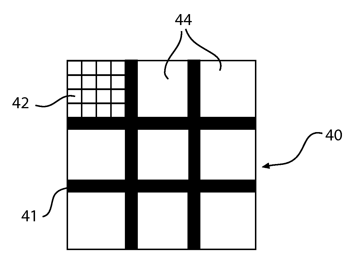
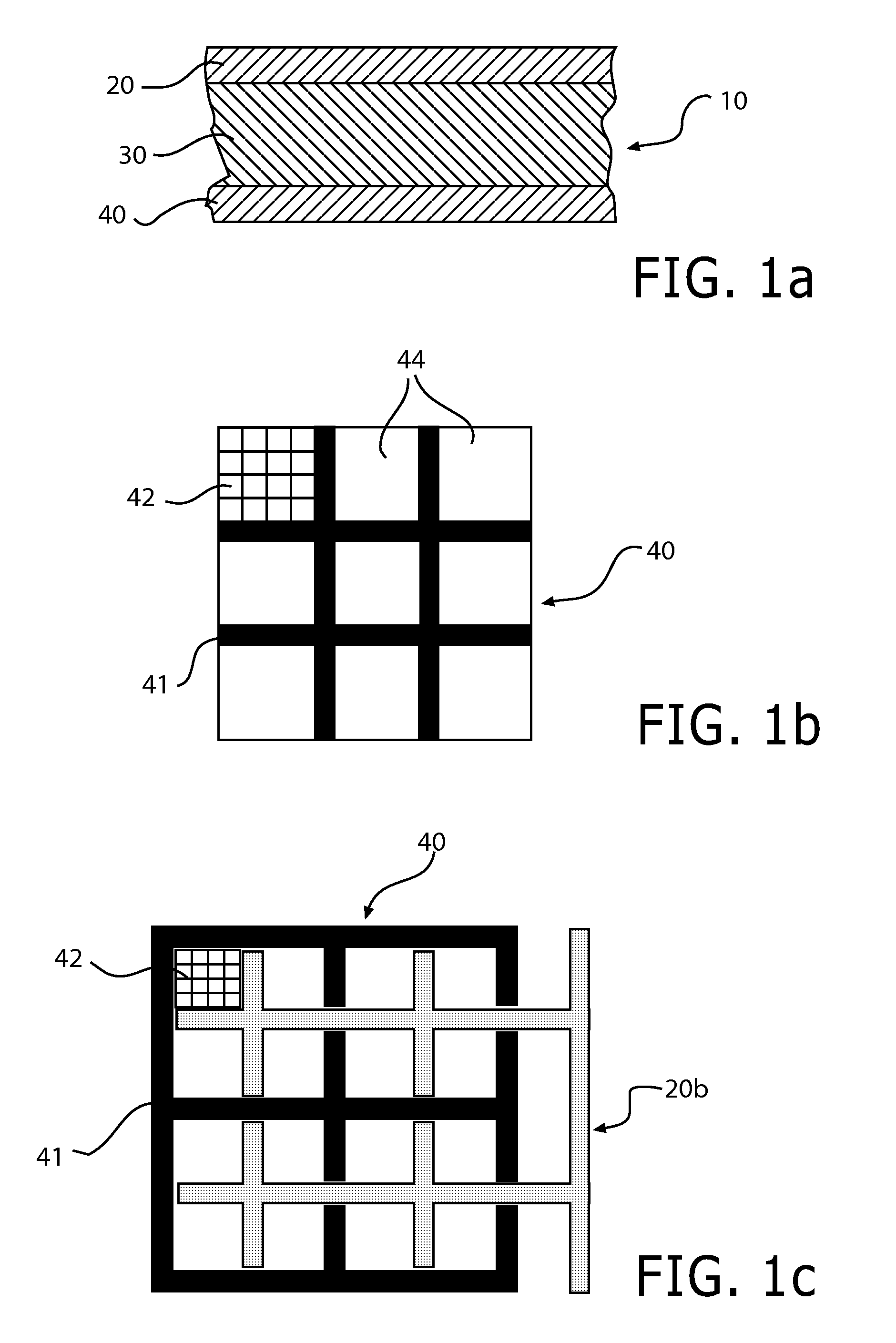
[0075]A basic aspect of the method is the manufacture of a certain layer of an electronic device, such as an OLED or an organic photovoltaic device (i.e. an organic solar cell), see FIG. 1a). The layer is a conducting layer, for instance the cathode layer 20 or the anode layer 40 of the OLED 10, which in other respects also contain several organic layers 30 between the anode and cathode layers 20, 40. The conducting layer can be regarded as an extra metallization, as has been described above in the background of the invention. The extra metallization is added to realise a current distribution layer that has a low resistivity and high open area. In practice this results in high aspect ration metal lines on the OLED 10.

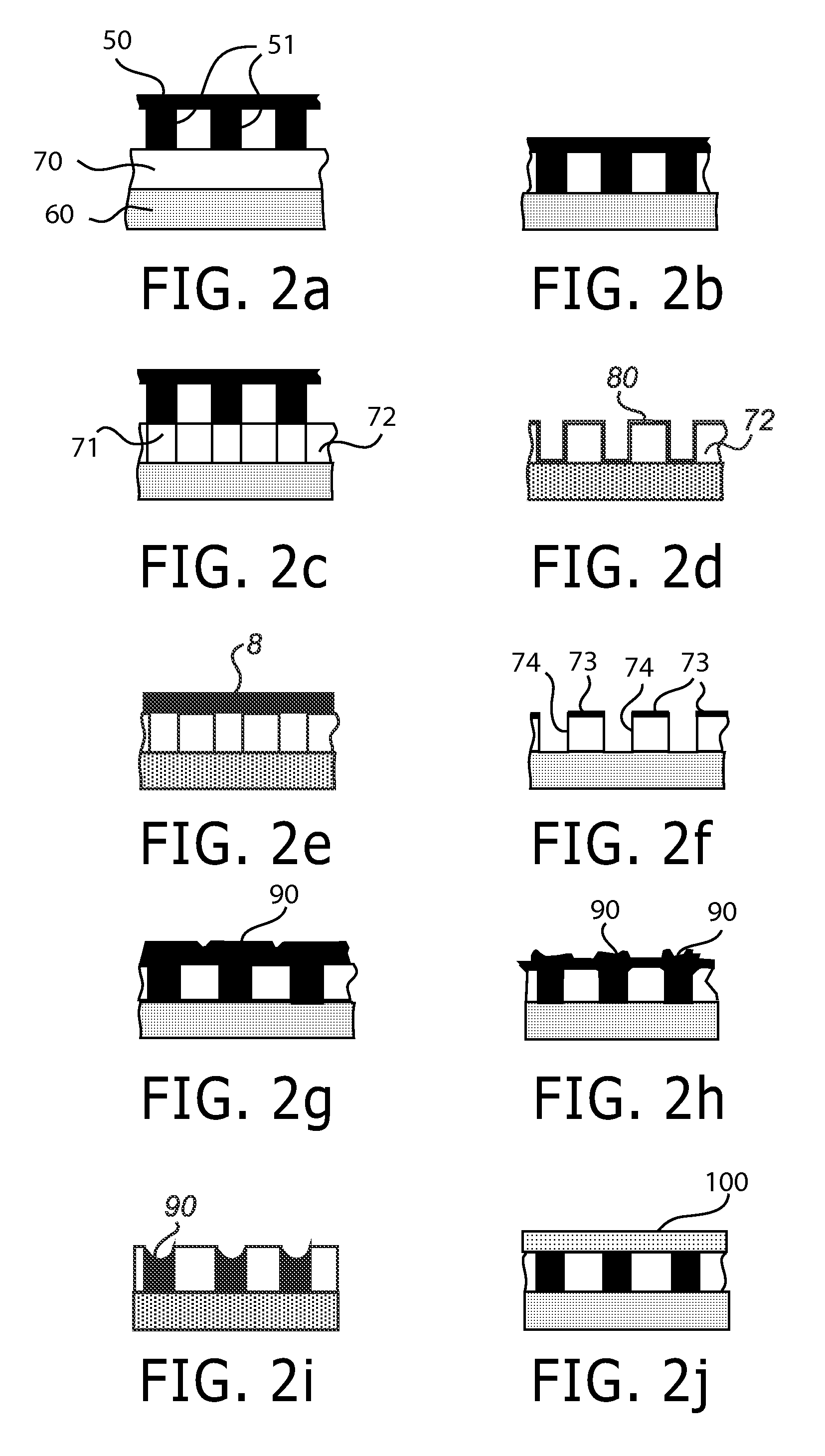
[0076]In the following the method according to the present invention is described in an non-limiting illustrative examp...


PUM

PropertyMeasurementUnit
sheet resistanceaaaaaaaaaa
aspect ratiosaaaaaaaaaa

Abstract

This invention relates to a method for forming a patterned layer on a substrate by means of an imprint process. According to the method a first layer is provided on the substrate, and a pattern of recesses is provided in the first layer by imprinting the layer with a patterning means. Then the first layer is cured. The curing is followed by performing a first surface treatment onto the first layer to make the surface of thereof hydrophilic, and then performing a second surface treatment onto a selected subarea of the surface of the first layer to make the. subarea hydrophobic. The subarea includes surface portions between the recesses and excludes the recesses. Finally, a conducting pattern material (41) is deposited into the recesses.

Description

FIELD OF THE INVENTION[0001]The present invention relates to a method for forming a patterned layer on a substrate and more particularly to a method for providing extra metallization to an organic light emitting device, OLED.BACKGROUND OF THE INVENTION[0002]Manufacturing methods based on organic semiconductor materials resulting in attractive applications like Organic Light Emitting Devices (OLEDs), also known as Organic Electroluminescent Devices (OELs), and photovoltaic devices (i.e. organic solar cells) are of great interest today. The main advantages of using organic materials are low cost and a capacity for large-area deposition, even on flexible substrates. Furthermore, the large variability of organic compounds allows tailoring the materials for specific applications.[0003]The OLED is a light-emitting device that typically consists of a number of organic layers which are based on small molecules and / or polymers and sandwiched between two electrodes, the anode and the cathode....

Claims


Application Information

Patent Timeline
Patent Type & Authority Patents(United States)
IPC IPC(8): B05D5/12H01L51/52H01L51/56H01L51/00H01L27/30
CPCH01L51/5206H01L51/5212H01L51/56H01L27/301H01L51/0021H01L2251/105H10K39/10H10K71/60H10K50/814H10K71/821H10K71/00H10K50/81
Inventor VERSCHUUREN, MARCUS ANTONIUSLIFKA, HERBERTTANASE, CRISTINA
Owner BEIJING XIAOMI MOBILE SOFTWARE CO LTD
Why Eureka
Try Eureka