

Organic electroluminescent element
a technology of electroluminescent elements and organic materials, applied in semiconductor devices, solid-state devices, diodes, etc., can solve the problems of limiting the device structure, limiting the method for realizing sufficient color rendering properties, and limiting the method. the effect of color rendering properties, high performance and long-li
- Summary
- Abstract
- Description
- Claims
- Application Information
AI Technical Summary
Benefits of technology
Problems solved by technology
Method used
Image

Examples
example 1
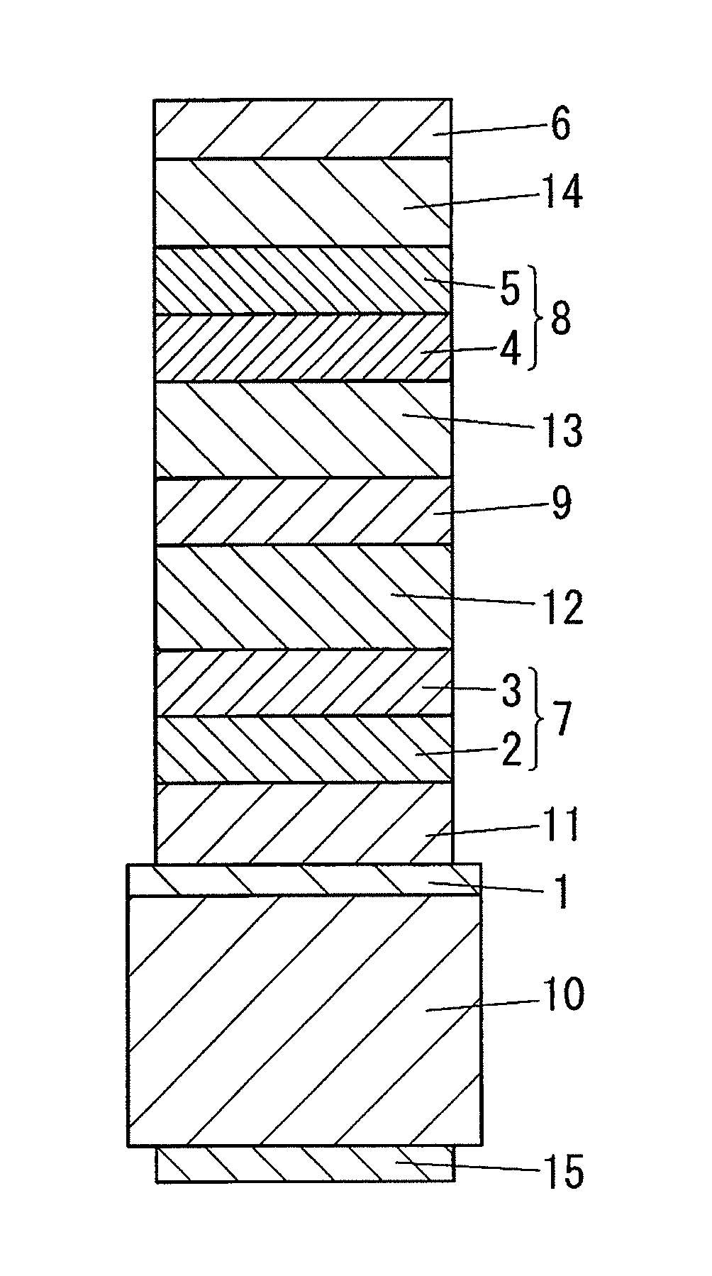
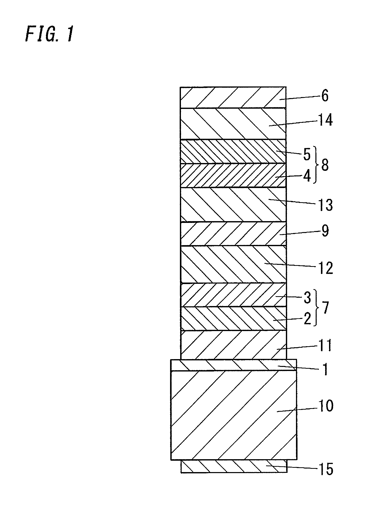
[0069]An organic electroluminescent element as shown in FIG. 1 was manufactured. Specifically, a transparent electrode 1 was formed by depositing ITO with a thickness of 130 nm on a substrate 10 (a glass substrate). A first hole transporting layer 11, a blue light-emitting layer 2 (containing BCzVBi, which is a fluorescent light-emitting material, as a blue light-emitting material), a first green light-emitting layer 3 (containing TPA, which is a fluorescent light-emitting material, as a first green light-emitting material) and a first electron transporting layer 4 were further formed by a vapor deposition method with a thickness between 5 nm and 60 nm and stacked on the transparent electrode 1 in this order. Next, an intermediate layer 9 having a layer structure of Alq3 / Li2O / Alq3 / HAT-CN6 was stacked with a layer thickness of 15 nm. Then, a second hole transporting layer 13, a red light-emitting layer 4 (containing Ir(piq)3, which is a phosphorescent light-emitting material, as a re...
example 2
[0078]An organic electroluminescent element having a multiunit structure as shown in FIG. 1 was manufactured. Specifically, a transparent electrode 1 was formed into a film by depositing ITO with a thickness of 130 nm on a substrate 10 (a glass substrate). A first hole transporting layer 11, a blue light-emitting layer 2 (containing BCzVBi, which is a fluorescent light-emitting material, as a blue light-emitting material), a first green light-emitting layer 3 (containing TPA, which is a fluorescent light-emitting material, as a first green light-emitting material) and a first electron transporting layer 4 were further formed by a vapor deposition method with a thickness between 5 nm and 60 nm and stacked on the transparent electrode 1 in this order. The blue light-emitting layer 2 and the first green light-emitting layer 3 constitute a fluorescent light-emitting unit 7. Next, an intermediate layer 9 having a layer structure of Alq3 / Li2O / Alq3 / HAT-CN6 was stacked with a layer thicknes...
PUM
 Abstract
Description
Claims
Application Information