Thermal package with heat slug for die stacks

a technology of heat slugs and die stacks, which is applied in the direction of electrical equipment, semiconductor devices, semiconductor/solid-state device details, etc., can solve the problems of increasing processor speeds, reducing the surface area available for dissipating heat, and reducing the size of dies in general. , to achieve the effect of improving heat dissipation and thermal connection, facilitating manufacturing, and facilitating device manufacturing

Inactive Publication Date: 2015-09-08
SONY MOBILE COMM AB +1
View PDF5 Cites 8 Cited by
  • Summary
  • Abstract
  • Description
  • Claims
  • Application Information

AI Technical Summary

Benefits of technology

[0006]It is an object of the invention to provide a semiconductor assembly, which solve, or at least mitigate, the problems with the heat impact in die stacking mentioned above.
[0007]Another object of the invention is to provide a semiconductor assembly that reduces the effect of excessive heat generation in active portions of dies by improved heat dissipation enabling dimensions of dies to be maintained or even reduced for less footprint area without increased heat impact and negative effects associated therewith.
[0008]Yet another object of the invention is to provide a semiconductor assembly that reduces the negative effects of its own heat generation compared to conventional die stacks as an increased heat generation and negative effects associated therewith does not have to be compensated for by “driving” / operating the co-operating active portions of the individual dies with lower performance similar to “dimming” down electric lights to save energy as in prior art die stacks, whereby better performance of the integrated circuits is achieved by the inventive semiconductor assembly having an optimized heat dissipation ability, i.e. a transient solution, and heat buffering, i.e. a sustainable solution, compared to known semiconductor assemblies.

Problems solved by technology

However, upper or outer vertical dies impede dissipation of heat from lower or inner dies or other components and prevalently increasing processor speeds may generate more heat than previous processors.
At the same time, the sizes of dies in general have been reduced, which reduces the surface area available for dissipating heat.

Method used


Image

  • Thermal package with heat slug for die stacks
  • Thermal package with heat slug for die stacks
  • Thermal package with heat slug for die stacks

Examples


first embodiment

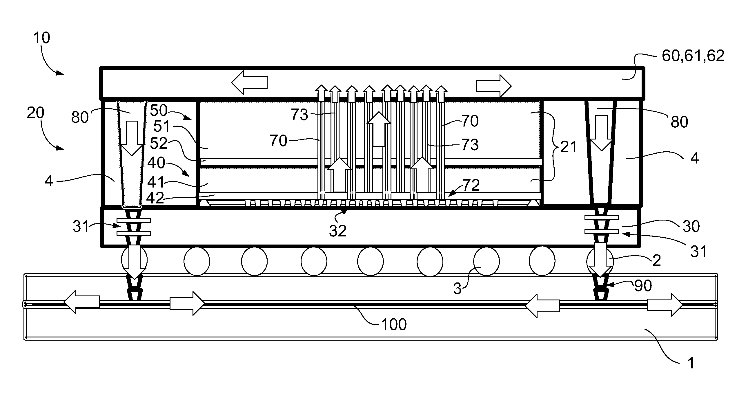
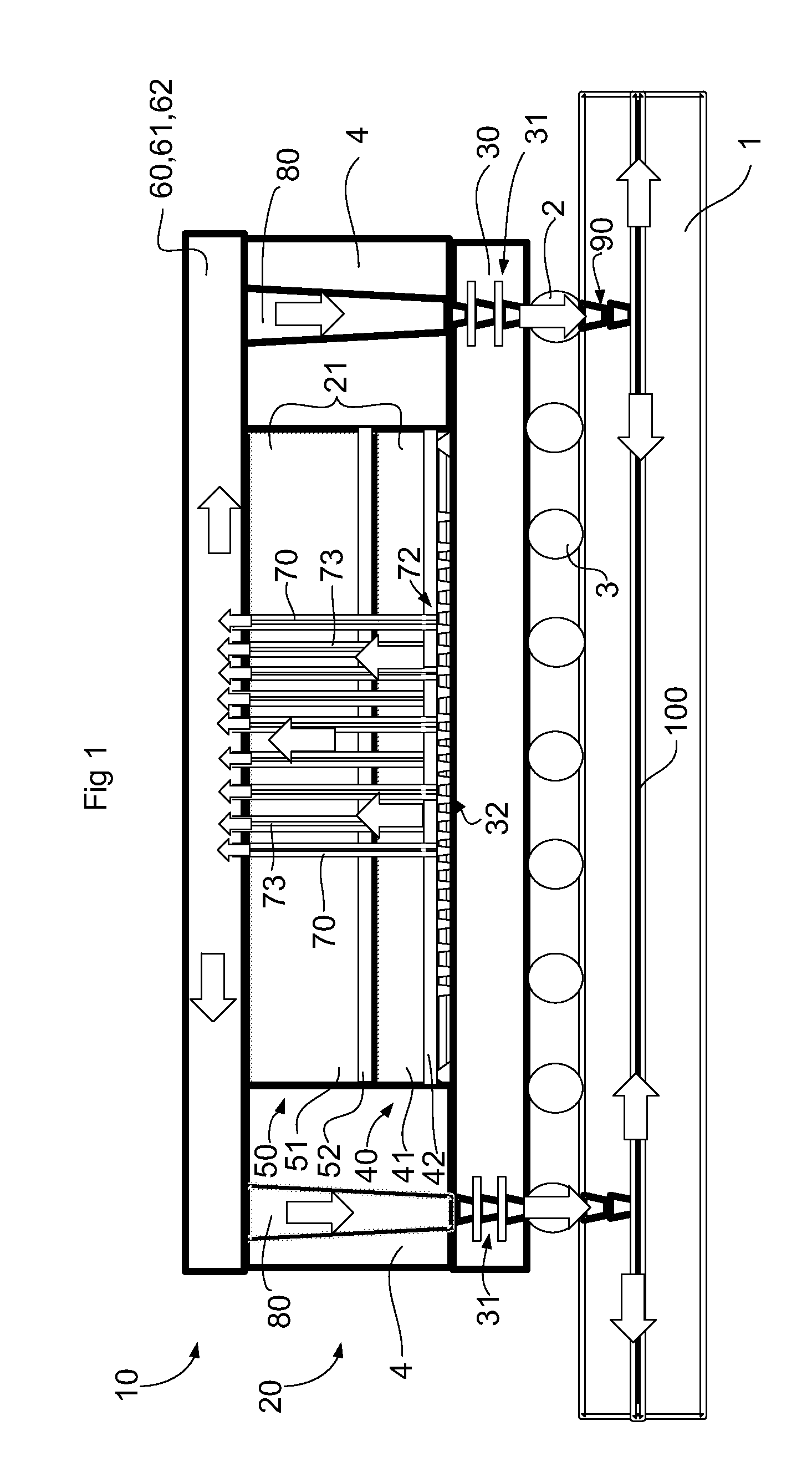
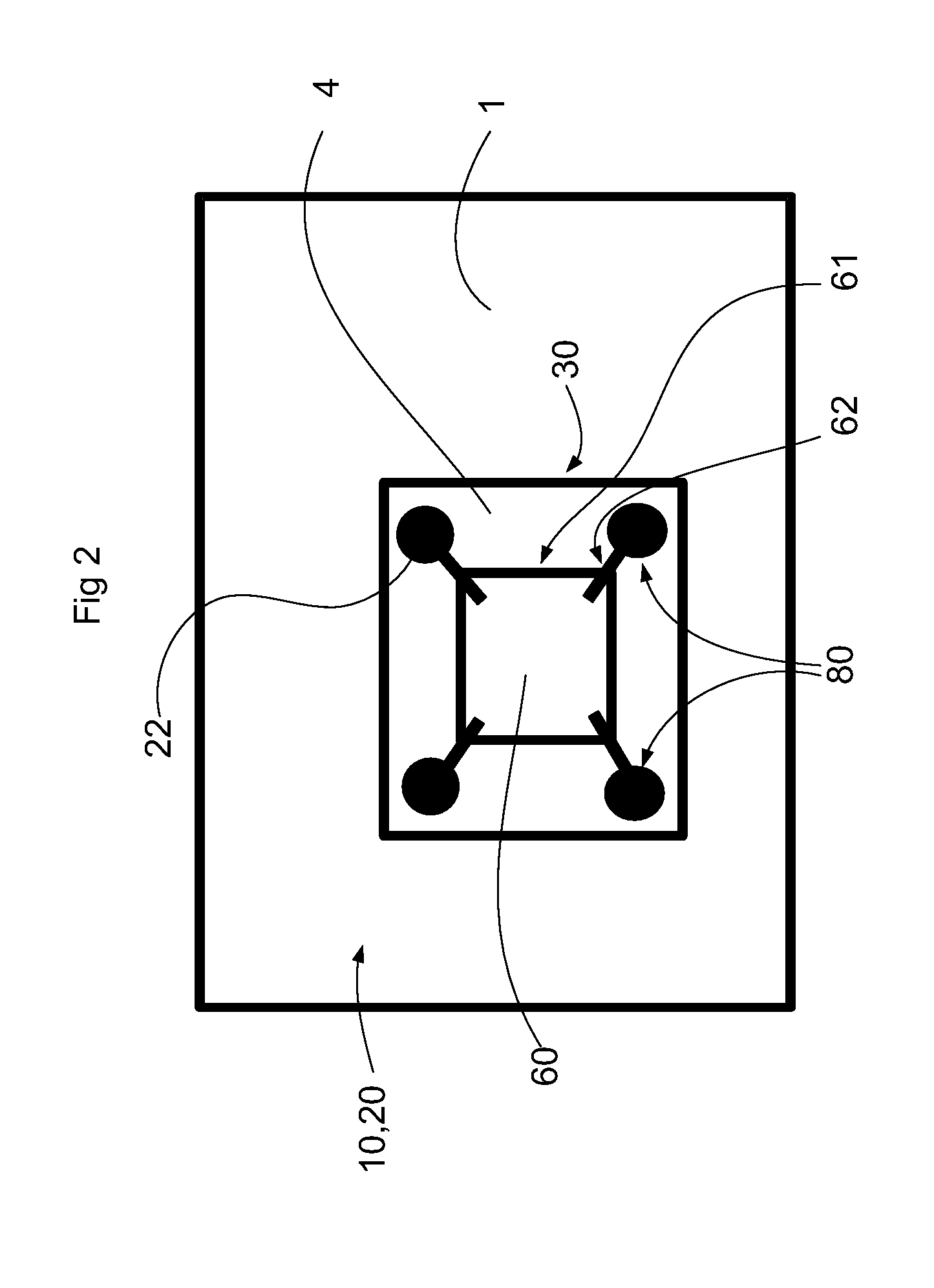
[0034]A semiconductor assembly 10 according to the invention is shown in FIGS. 1 to 4, wherein like reference numerals designate corresponding or similar elements throughout the views, a semiconductor assembly 10 is shown in FIG. 1. A package 20 comprising a die stack 21 is included in the semiconductor assembly 10 and may have a die-die connection using a Micro Pillar Grid Array (MPGA) in the package. The die stack 21 comprising dies 40, 50, the package 20 and a printed circuit / wiring board 1 are operatively connected in a known way by solder joints 2, which connections will not be explained in detail as the skilled person is aware of this technique.

[0035]The die stack 21 includes a first die / an lower die 40, at least one further / second / upper die 50, and a package substrate 30. The dies disclosed herein are semiconductors that may have passive portions 41, 51, active portions 42, 52 or any combination or number of such portions depending on the desired function and application of t...

second embodiment

[0044]The dies 40, 50 of the semiconductor assembly 10 and the others described herein may be made based on silicon (Si) and variants thereof. In some cases for example germanium (Ge) or Ge and carbon are added to Si to increase charge carrier mobility. Alternative materials may include but not be limited to gallium arsenide (GaAs), indium phosphide (InP), graphene, or other III-IV semiconductor compounds. Further, although Through-Silicon Vias are referred to herein as TSV:s because of the prevalence of the use of silicon, in light of the fact that other materials may be used for the die, the term TSV is understood to apply to a like passage regardless of the die material In the embodiment shown in FIGS. 1-4, the upper die 50 may be, for example, a DRAM, and the lower die 40 may be a CPU die. However, various components may be used in such an arrangement, including but not limited to stacking of processor blocks. In a semiconductor assembly 10 shown in FIG. 4, a package 200 include...


PUM


Abstract

A semiconductor assembly comprises a package, which in turn comprises at least one substrate, a first die stacked onto the substrate, at least one further die stacked onto the first die, at least one heat spreader in the package, and TSV:s extending through the stacked dies. The ends of the TSV:s are exposed at the further die.

Description

CROSS-REFERENCE TO RELATED APPLICATION[0001]This application claims the benefit of U.S. Provisional Patent Application Ser. No. 61 / 635,376, filed Apr. 19, 2012, the entire disclosure of which is hereby incorporated by reference.[0002]The present invention relates to integrated circuits and associated electronics, and particularly to heat dissipation features of vertically stacked dies in packages and other printed board assemblies.BACKGROUND ART[0003]In three dimensional packaging, connected integrated circuits are made more compact by vertically stacking two or more dies with a high speed and substantially direct interface. The main reason for vertically stacking dies is better signal performance, i.e. stacked dies are less parasitic as wire length is reduced. Micro ball connections that may be used with vertical die stacks instead of relatively long leads on the periphery of the chips may reduce elapsed time for communication of signals between components, thus increasing speed as...

Claims


Application Information

Patent Timeline
Patent Type & Authority Patents(United States)
IPC IPC(8): H01L23/34H01L29/40H01L23/52H01L23/48H01L23/02H01L23/28H01L25/065H01L23/433H01L23/373H01L23/367H01L23/36
CPCH01L23/34H01L23/36H01L23/3677H01L23/3735H01L23/4334H01L25/0657H01L2224/16225H01L2224/32225H01L2224/73204H01L2225/06513H01L2225/06517H01L2225/06541H01L2225/06565H01L2225/06589H01L2924/15311H01L2924/00
Inventor LUNDBERG, NILS
Owner SONY MOBILE COMM AB
Why Eureka
Try Eureka