Check patentability & draft patents in minutes with Patsnap Eureka AI!

Method and system for measuring bumps based on phase and amplitude information

a technology of phase and amplitude information, applied in the direction of instruments, material analysis, computer peripheral equipment, etc., can solve the problems of noisy phase information, more severe noise, and noisy phase measurement process

Inactive Publication Date: 2015-09-29
CAMTEK LTD
View PDF45 Cites 1 Cited by
  • Summary
  • Abstract
  • Description
  • Claims
  • Application Information

AI Technical Summary

Benefits of technology

This approach enables fast and accurate height measurement of microscopic structures beyond the limitations of traditional methods, reducing errors and extending the measurable height range.

Problems solved by technology

It is known in the art that the measurement of phase is a noisy process and that phase information is noisy.
This noise can be more severe when measuring structures such as bumps due to their shape.
Such methods are not applicable to bump metrology due to intrinsic phase discontinuity due to bump geometry.
When operating at there discontinuities the height measurement will suffer from possible errors as small noises can result in a very large offset in the height measurement.

Method used


Image

  • Method and system for measuring bumps based on phase and amplitude information
  • Method and system for measuring bumps based on phase and amplitude information
  • Method and system for measuring bumps based on phase and amplitude information

Examples


first embodiment

[0053]Phase noise is illustrated by FIGS. 5a and 5b that include different phase information (phase images 52 and 54) for the same bump—as they were taken at different points of time but while applying the same illumination and collection conditions.

[0054]Phase information can be processed to extract pixels that may be noisier then other pixels—or at least are expected to include too much noise.

[0055]A method is provided and may include singling out the significant pixel (or pixels) out of phase information pixels.

[0056]The entire bump phase information can be processed to choose phase information pixels that share the same attribute values such as have similar statistical qualities as the significant pixels.

[0057]The height of the bump can be determined based upon these found out pixels.

[0058]The method may start by defining or receiving (62) an amplitude threshold. The amplitude threshold can be either set by user or automatically learned from frame

[0059]The selection process may ...

second embodiment

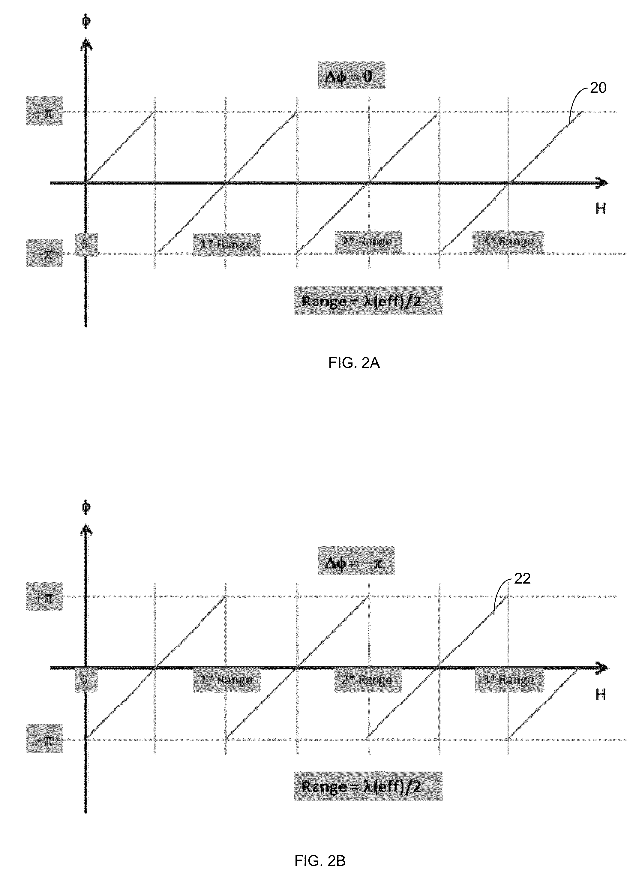
[0077]For any semiconductor process there is an expected (nominal) bump height (H0) as well as expected tolerances that the bump height. These tolerances can be represented by minimal and maximal tolerable heights (Hmin, and Hmax). Also, there is an expected relationship (diameter to height ratio) between the diameter of a bump and the height of the bump.

[0078]It is noted that a combination of the second and first embodiments can be provided. For example, method 30 can be executed on pixels that are selected by method 60. Yet for another example, the devices of FIGS. 4 and 8 can be combined.

[0079]FIG. 3 illustrates a method 30 for determining a height of a bump according to an embodiment of the invention.

[0080]Method 30 starts by initialization stage 31. The initialization stage may include receiving an expected height of the bump, and receiving expected relationships between diameter values and height values of bumps. This information is usually provided by the manufacturer of the ...


PUM

PropertyMeasurementUnit
heightaaaaaaaaaa
sizeaaaaaaaaaa
amplitude thresholdaaaaaaaaaa

Abstract

A method and device for measuring a height of a microscopic structure such as solder bumps. For simplicity of explanation, the invention is described with respect to phase information and amplitude information wherein phase detection and calculation algorithms are being used.

Description

BACKGROUND OF THE INVENTION[0001]Electrical circuits and other samples may include multiple microscopic structures such as bumps that should be measured for various purposes.[0002]FIG. 1 illustrates a prior art portion 10 of a semiconductor chip with multiple solder bumps.[0003]A bump has a shape that may be approximated by a dome. The manufacturing process of the bump mandates certain height to diameter ratios of the bump.[0004]There are several known optical height metrology methods. The most sensitive methods are based on phase detection using various interferometric principles.[0005]It is known in the art that the measurement of phase is a noisy process and that phase information is noisy. This noise can be more severe when measuring structures such as bumps due to their shape.[0006]Digital holographic microscopes such as the DHM R1100™ of Lyncee Tec of Lausanne Switzerland use two laser sources that can be simultaneously or alternatively switched or continuously operate to illu...

Claims


Application Information

Patent Timeline
Patent Type & Authority Patents(United States)
IPC IPC(8): G06K9/32G06K9/00G02B21/00G01N21/956G01B11/06
CPCG06K9/00127G01N21/95607G01N21/95684G02B21/0016G01B11/0608G02B21/0056G06V20/69G01B11/24G01B9/02
Inventor KOREN, SHIMONSHUR, ORMALINOVICH, YACOVGOLAN, GILAD
Owner CAMTEK LTD
Features
  • R&D
  • Intellectual Property
  • Life Sciences
  • Materials
  • Tech Scout
  • Unparalleled Data Quality
  • Higher Quality Content
  • 60% Fewer Hallucinations
Learn More