Electromagnetic wave propagation path and electromagnetic wave propagation device

a propagation path and electromagnetic wave technology, applied in coupling devices, electrical devices, waveguides, etc., can solve the problems of destabilizing communication quality, reducing cost, and reducing the effort of downsizing electronic devices, and achieves low loss, low leakage characteristics, and high resistance to interference waves.

Inactive Publication Date: 2014-06-19
HITACHI LTD
View PDF2 Cites 226 Cited by
  • Summary
  • Abstract
  • Description
  • Claims
  • Application Information

AI Technical Summary

Benefits of technology

[0012]The electromagnetic wave propagation device according to the present invention allows branching extension of the propagation path with low loss while keeping the low leakage characteristic an...

Problems solved by technology

Similarly, in the housing of the electronic apparatus, the numbers of modules that constitute the electronic apparatus, and the wiring cords among the electronic components have been increasing, which interferes with the effort of downsizing the electronic apparatus, reducing the cost, and improving reliability.
However, there may be a concern that the metal wall surface of the housing in the wireless communication system irregularly reflects the electromagnetic wave, thus destabilizing communication quality.
The general...

Method used


Image

  • Electromagnetic wave propagation path and electromagnetic wave propagation device
  • Electromagnetic wave propagation path and electromagnetic wave propagation device
  • Electromagnetic wave propagation path and electromagnetic wave propagation device

Examples


first embodiment

[0041]A first embodiment according to the present invention will be described referring to FIGS. 1A to 3.

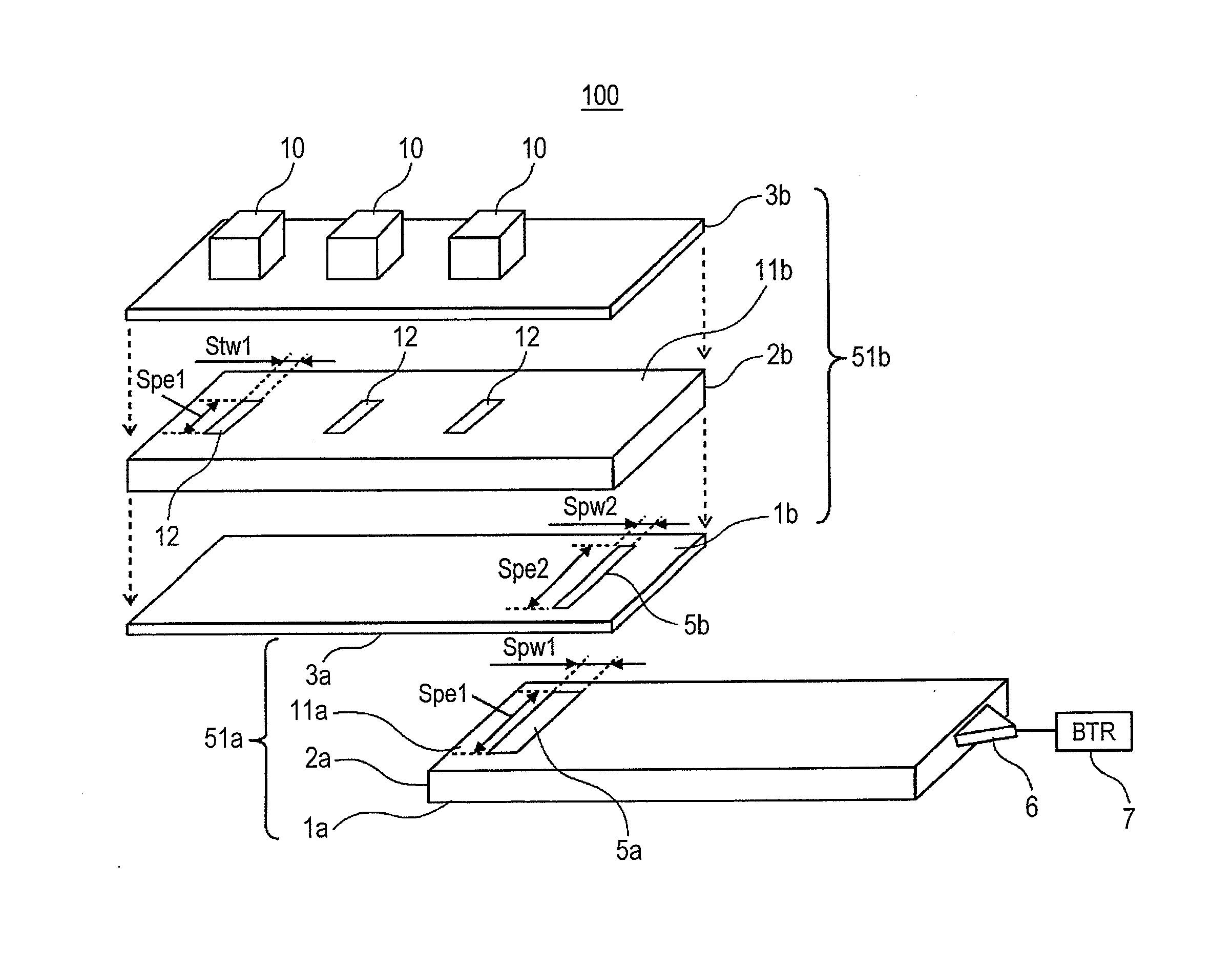
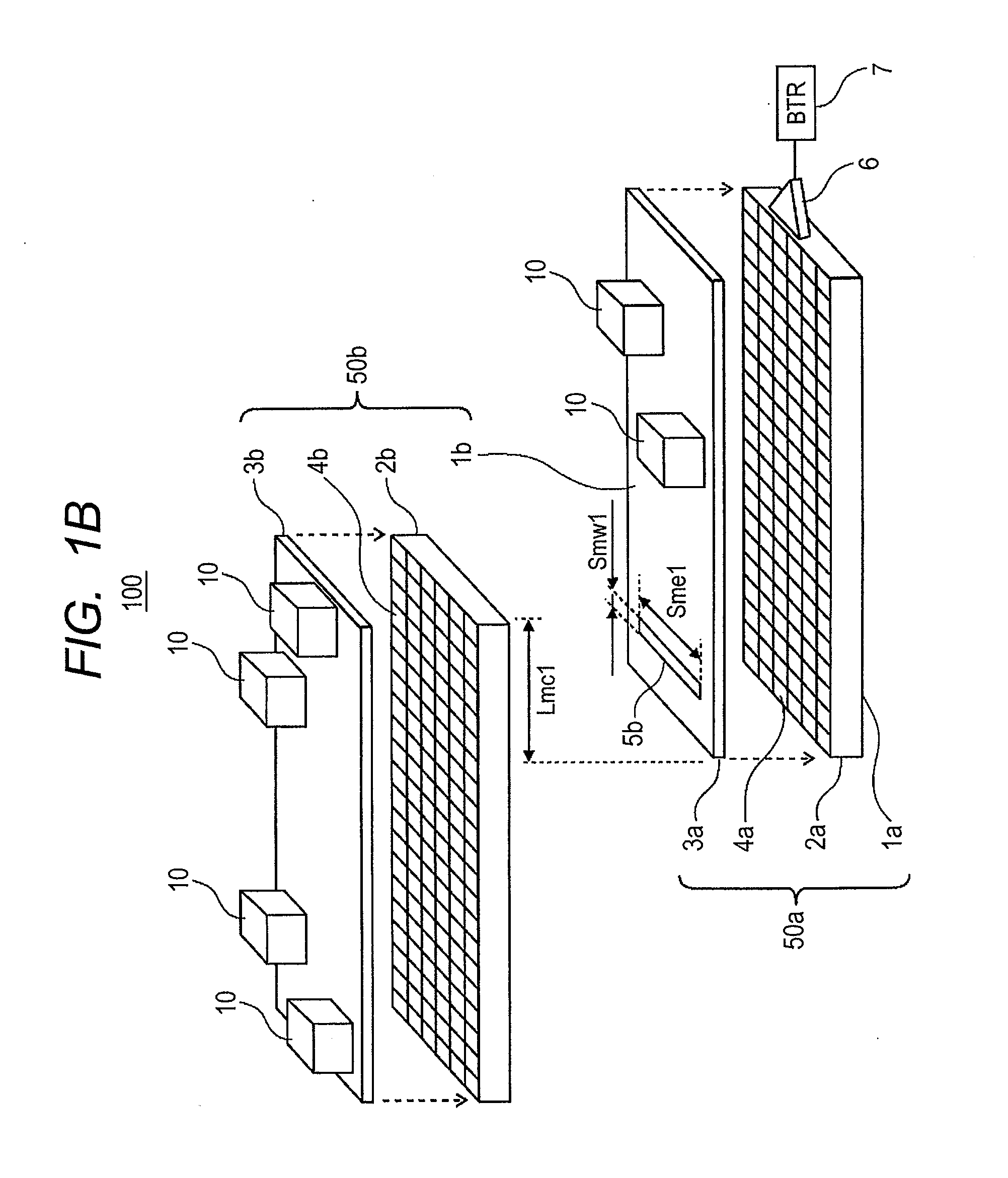
[0042]FIG. 1A illustrates an example of an electromagnetic wave linking unit for two planar propagation media that form an electromagnetic wave propagation path of an electromagnetic wave propagation device according to the first embodiment. FIG. 1B is an exploded perspective view of major surfaces of the electromagnetic wave propagation device for easy understanding of the structure.

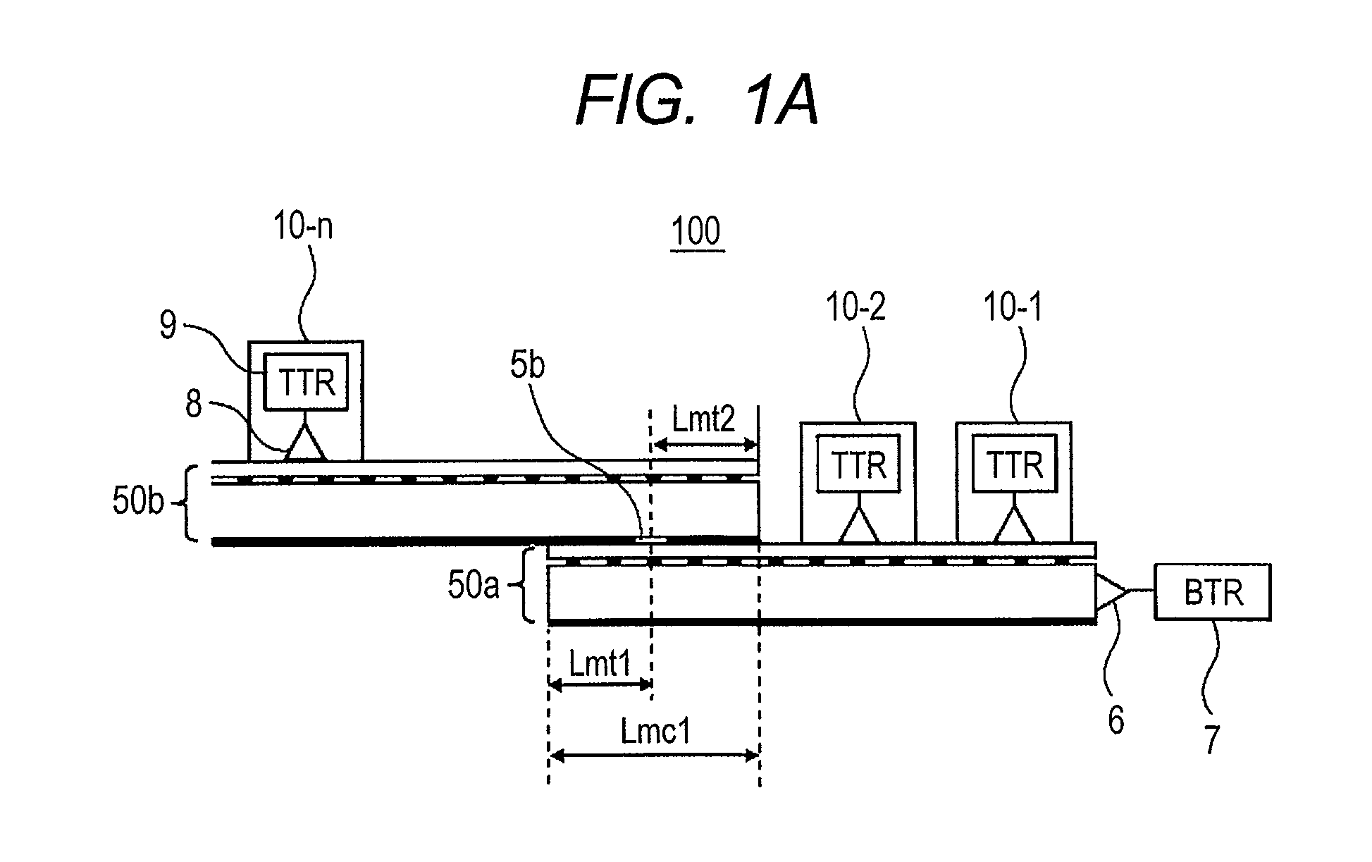
[0043]An electromagnetic wave propagation device 100 is a device for transmitting and receiving information between at last one communication base station 7 and multiple communication terminals 10 (10-1 to 10-n), which includes planar propagation media 50a, 50b, and a parallel transformation type interface 6. The respective communication terminals 10 are transceivers installed in the multiple electronic apparatuses as communication modules for communication with the communication base station 7. Freq...

second embodiment

[0068]A second embodiment according to the present invention will be described referring to FIGS. 4 to 9.

[0069]FIG. 4 is a sectional view of the electromagnetic wave linking unit for the planar propagation media of the electromagnetic wave propagation device according to the second embodiment.

[0070]The electromagnetic wave propagation device 100 serves to transmit and receive information between the communication base station 7 and the communication terminals 10, and includes planar propagation media 51a, 51b, and the parallel transformation type interface 6.

[0071]The two planar propagation media 50a, 50b are disposed to have the respective regions around end portions partially superposed while having the obverse face of the medium and the reverse face of the other medium overlapped. The electromagnetic linking unit is provided at the overlapped part to form the propagation path for the electromagnetic wave as the communication signal. It is assumed that the distance of the overlapp...

third embodiment

[0093]A third embodiment according to the present invention will be described referring to FIGS. 10 to 13.

[0094]FIG. 10 is a sectional view showing a structure of the electromagnetic wave propagation device 100 according to the third embodiment. The electromagnetic wave propagation device 100 serves to transmit and receive information between the communication base station 7 and the communication terminals 10, and includes the planar propagation media 52a, 52b, and the parallel transformation type interface 6.

[0095]The two planar propagation media 52a and 52b are partially overlapped (distance of the overlapped part=Lrt1). They are provided with the electromagnetic wave linking unit including a sparse mesh conductor 13a with a mesh pitch larger than that of the planar mesh conductor 4a at the non-overlapped part provided for the medium 52a, and a sparse mesh conductor 13b provided for the planar conductor 1b of the medium 52b. This makes it possible to connect the two planar propaga...


PUM


Abstract

An electromagnetic wave propagation device includes multiple planar propagation media each formed by laminating at least one planar conductor and at least one planar dielectric, multiple transceivers for transmitting and receiving information among electronic apparatuses, and a first interface for transmitting and receiving the electromagnetic wave between the transceivers and the planar propagation media. Planar dielectric spacers are provided for isolating the multiple planar propagation media from one another. The planar propagation medium is disposed to have an overlapped part with at least the other of the planar propagation media so that an obverse face of the medium and a reverse face of the other medium are at least partially overlapped with each other. The planar conductor is provided with an electromagnetic wave linking unit at the overlapped part that transmits and receives the electromagnetic wave between the planar propagation media.

Description

TECHNICAL FIELD[0001]The present invention relates to an electromagnetic wave propagation path and an electromagnetic wave propagation device, and more specifically, to an electromagnetic wave propagation path and an electromagnetic wave propagation device which employ planar propagation media for propagating electromagnetic waves, and are suitable for three-dimensional branching extension.BACKGROUND ART[0002]The recent advancement of networking electronic apparatuses in various fields of consumer and social infrastructures shows the trend of significant increase in the number of wiring cords for connecting those electronic apparatuses. Similarly, in the housing of the electronic apparatus, the numbers of modules that constitute the electronic apparatus, and the wiring cords among the electronic components have been increasing, which interferes with the effort of downsizing the electronic apparatus, reducing the cost, and improving reliability.[0003]Introduction of the generally emp...

Claims


Application Information

Patent Timeline
IPC IPC(8): H01P5/12
CPCH01P3/023H01P5/028H01P5/12
Inventor SHINODA, HIROSHITERADA, TAKAHIDEHARA, KAZUNORI
Owner HITACHI LTD
Why Eureka
Try Eureka