Method of manufacturing semiconductor device, method of processing substrate and non-transitory computer readable recording medium

a semiconductor and recording medium technology, applied in the direction of liquid surface applicators, coatings, chemical vapor deposition coatings, etc., can solve the problems of reducing the yield, lowering the yield, and reducing the number of substrates that are processed when substrate processing is performed once, so as to reduce the yield and increase the pitch of the substrate arrangement. , the effect of lowering the yield

Active Publication Date: 2015-11-17
KOKUSA ELECTRIC CO LTD
View PDF14 Cites 332 Cited by
  • Summary
  • Abstract
  • Description
  • Claims
  • Application Information

AI Technical Summary

Benefits of technology

[0008]The present invention provides a method of manufacturing a semiconductor device capable of improving the yield of a film by improving the thickness uniformity or step coverage of an insulating film having a stacked structure of an oxide film and a nitride film, a method of processing the substrate, a substrate processing apparatus, and a non-transitory computer-readable recording medium.

Problems solved by technology

However, if the former method of lowering the pressure in the process chamber is used, a deposition rate of the insulating film may decrease, thus lowering the yield.
If the latter method of increasing the pitch of substrate arrangement is used, the number of substrates that are processed when substrate processing is performed once may decrease, thereby greatly lowering the yield.

Method used


Image

  • Method of manufacturing semiconductor device, method of processing substrate and non-transitory computer readable recording medium
  • Method of manufacturing semiconductor device, method of processing substrate and non-transitory computer readable recording medium
  • Method of manufacturing semiconductor device, method of processing substrate and non-transitory computer readable recording medium

Examples


first modified example

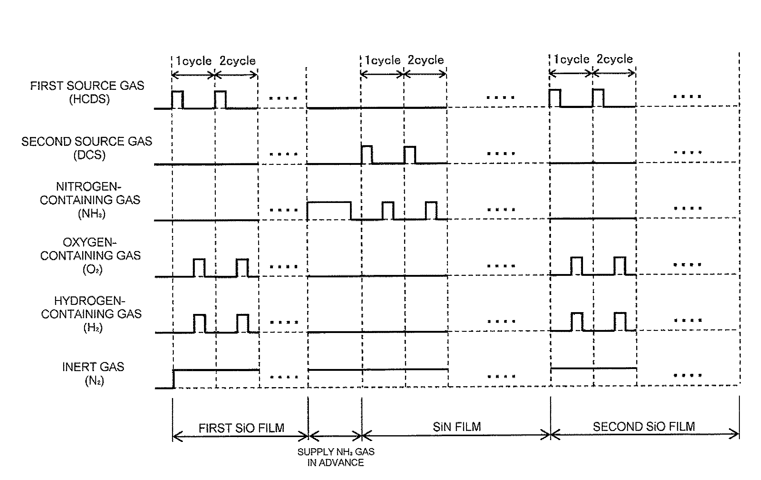
[0188]Although in film-forming sequence illustrated in FIGS. 4 and 11, a first source gas used to form a first oxide film or a second oxide film and a second source gas used to form a nitride film are different types of source gases, the first modified example is not limited thereto. For example, the first source gas and the second source gas may be formed of the same material.

[0189]FIG. 5 is a flowchart illustrating a method of forming a film according to the first modified example of the first embodiment of the present invention. FIG. 12 is a gas supply timing chart according to the first modified example of the first embodiment of the present invention. FIGS. 5 and 12 illustrate cases in which HCDS gas is used as both a first source gas and a second source gas. The film-forming sequence according to the first modified example is the same as those of FIGS. 5 and 12, except that the HCDS gas is used as the second source gas in forming a nitride film. Forming a nitride film (or sili...

second modified example

[0201]In the film-forming sequence illustrated in FIGS. 4 and 11, the first oxide film and the second oxide film are formed by repeatedly performing a cycle including supplying a first source gas and supplying an oxygen-containing gas and a hydrogen-containing gas, several times, but a second modified example is not limited thereto.

[0202]For example, in forming a first oxide film and / or forming a second oxide film, a cycle including supplying a first source gas and supplying an oxygen-containing gas and a hydrogen-containing gas may be repeatedly performed several times, and then supplying the oxygen-containing gas and the hydrogen-containing gas (modification process) may be performed. In this film-forming sequence, the oxygen-containing gas and the hydrogen-containing gas are thermally activated and supplied without using plasma, as in the film-forming sequence described above with reference to FIGS. 4 and 11. Also, this film-forming sequence may be performed using at least one of...

third and fourth modified examples

[0208]In the film-forming sequence described above with reference to FIGS. 4 and 11, the first and second oxide films are formed by repeatedly performing a cycle including the process of supplying the first source gas and the process of supplying the oxygen-containing gas and the hydrogen-containing gas, several times, but third and fourth modified examples of the first embodiment of the present invention are not limited thereto.

[0209]For example, in forming a first oxide film and / or forming a second oxide film, supplying a first source gas may be skipped, and instead, an oxygen-containing gas and a hydrogen-containing gas may be continuously supplied. Also, film-forming sequences according to the third and fourth modified examples may be performed using at least one of the process of forming the first oxide film and the process of forming the second oxide film.

[0210]FIG. 7 is a flowchart illustrating a method of forming a film according to the third modified example of the first em...


PUM

PropertyMeasurementUnit
timeaaaaaaaaaa
timeaaaaaaaaaa
pressureaaaaaaaaaa

Abstract

A semiconductor manufacturing method includes forming an oxide film on a substrate by performing a first cycle a predetermined number of times, including supplying a first source gas, an oxidizing gas and a reducing gas to the substrate heated to a first temperature in a process container under a sub-atmospheric pressure; forming a seed layer on a surface of the oxide film by supplying a nitriding gas to the substrate in the process container, the substrate being heated to a temperature equal to or higher than the first temperature and equal to or lower than a second temperature; and forming a nitride film on the seed layer formed on the surface of the oxide film by performing a second cycle a predetermined number of times, including supplying a second source gas and the nitriding gas to the substrate heated to the second temperature in the process container.

Description

CROSS-REFERENCE TO RELATED PATENT APPLICATION[0001]This U.S. non-provisional patent application claims priority under 35 U.S.C. §119 of Japanese Patent Application No. 2011-218019, filed on Sep. 30, 2011, and Japanese Patent Application No. 2012-176570, filed on Aug. 9, 2012, in the Japanese Patent Office, the entire contents of which are hereby incorporated by reference.BACKGROUND OF THE INVENTION[0002]1. Field of the Invention[0003]The present invention relates to a method of manufacturing a semiconductor device, which includes forming a thin film on a substrate, a method of processing the substrate, a substrate processing apparatus that may be used in the process of forming the thin film, and a non-transitory computer-readable recording medium.[0004]2. Description of the Related Art[0005]As one process of a method of manufacturing a semiconductor device, forming an insulating film having an ONO stacked structure, in which an oxide film and a nitride film are alternately stacked o...

Claims


Application Information

Patent Timeline
Patent Type & Authority Patents(United States)
IPC IPC(8): H01L21/31H01L21/02H01L21/67C23C16/34C23C16/40C23C16/455
CPCH01L21/022C23C16/345C23C16/402C23C16/45529H01L21/0217H01L21/0228H01L21/0262H01L21/02164H01L21/02211H01L21/02532H01L21/67109H01L21/0254H01L21/324
Inventor YUASA, KAZUHIROAKAE, NAONORITERASAKI, MASATO
Owner KOKUSA ELECTRIC CO LTD
Why Eureka
Try Eureka