Semiconductor device and driving method thereof

a technology of semiconductor devices and drives, applied in the direction of fault response, redundant data error correction, instruments, etc., can solve the problem that the expected value (data based on the remainder) might be changed, and achieve the effect of high accuracy

Active Publication Date: 2016-01-05
SEMICON ENERGY LAB CO LTD
View PDF139 Cites 4 Cited by
  • Summary
  • Abstract
  • Description
  • Claims
  • Application Information

AI Technical Summary

Benefits of technology

[0010]An object of one embodiment of the present invention is to provide a semiconductor device in which a CRC is performed without soft errors. In other words, an object of one embodiment of the present invention is to provide a semiconductor device in which an error is detected with high accuracy.
[0011]Another object of one embodiment of the present invention is to provide a method for driving a semiconductor device in which a CRC is performed without soft errors. In other words, another object of one embodiment of the present invention is to provide a method for driving a semiconductor device in which an error is detected with high accuracy.
[0019]It is possible to provide a semiconductor device in which a CRC can be performed without soft errors, namely, a semiconductor device in which an error is detected with high accuracy.

Problems solved by technology

However, since the remainder is stored in the volatile memory (such as an SRAM), an expected value (data based on the remainder) might be changed due to soft errors.

Method used


Image

  • Semiconductor device and driving method thereof
  • Semiconductor device and driving method thereof
  • Semiconductor device and driving method thereof

Examples


embodiment 1

(Embodiment 1)

[0029]A configuration of a memory element which can be used for a semiconductor device of one embodiment of the present invention, and the operation thereof will be described.

[0030]Note that the description in this embodiment is made focusing on one memory element; however, in an actual semiconductor device, a plurality of memory elements are arranged in a matrix.

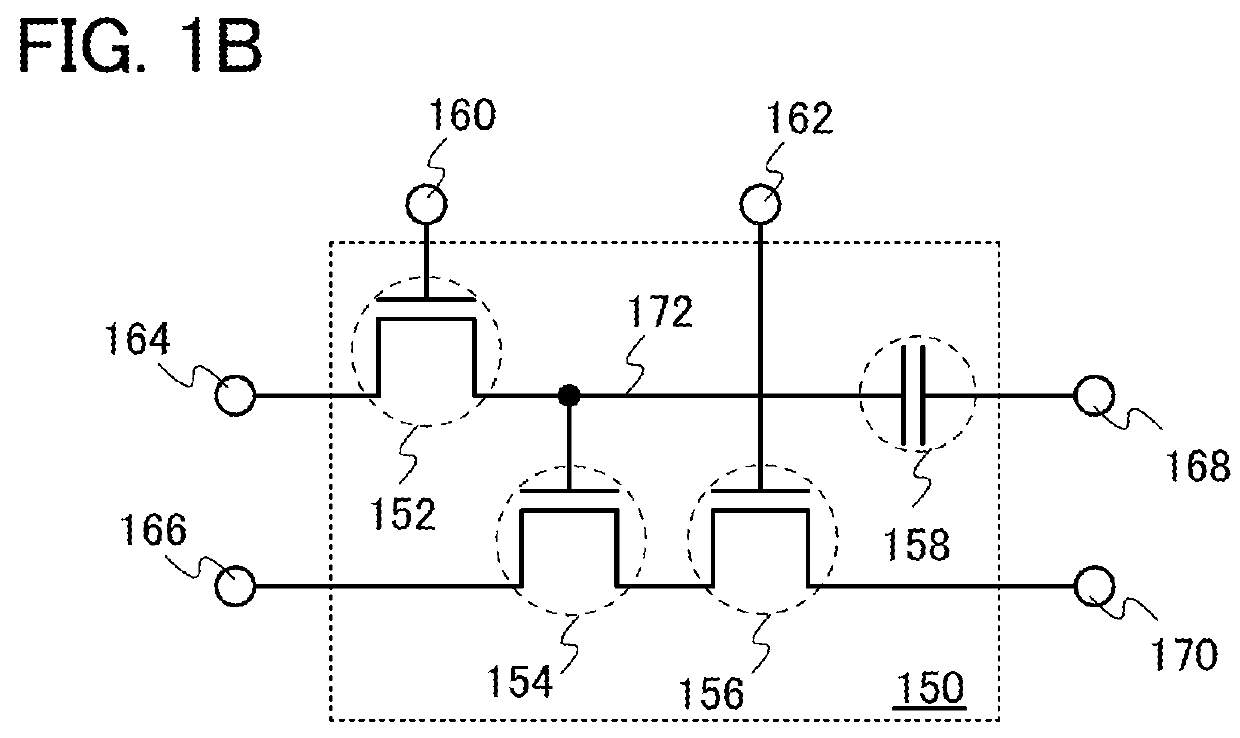
[0031]FIG. 1A illustrates an example of the configuration of the memory element that can be used for the semiconductor device of one embodiment of the present invention. A memory element 100 illustrated in FIG. 1A includes a first transistor 102, a second transistor 104, a capacitor 106, and a data storage portion 118, and is electrically connected to a first terminal 108, a second terminal 110, a third terminal 112, a fourth terminal 114, and a fifth terminal 116.

[0032]One of a source and a drain of the first transistor 102 is electrically connected to the third terminal 112. The other of the source and the d...

embodiment 2

(Embodiment 2)

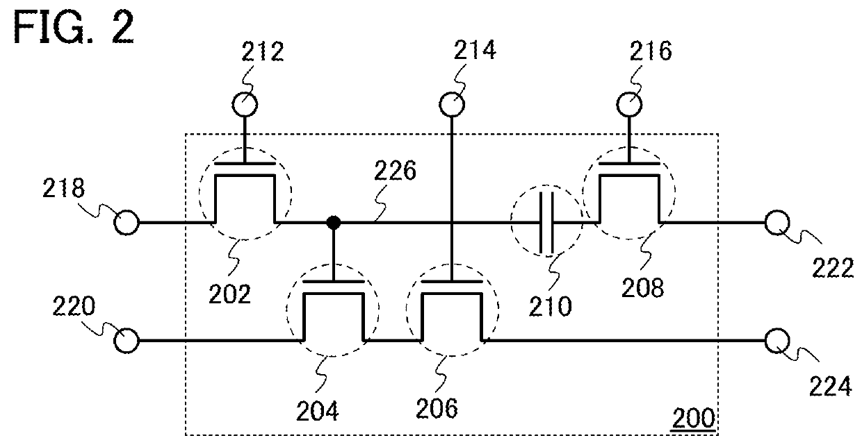
[0056]FIG. 2 illustrates an example of the configuration of the memory element that can be used for the semiconductor device of one embodiment of the present invention, which is different from those of FIGS. 1A and 1B. A memory element 200 illustrated in FIG. 2 includes a first transistor 202, a second transistor 204, a third transistor 206, a fourth transistor 208, a capacitor 210, and a data storage portion 226, and is electrically connected to a first terminal 212, a second terminal 214, a third terminal 216, a fourth terminal 218, a fifth terminal 220, a sixth terminal 222, and a seventh terminal 224.

[0057]The first transistor 202 has a structure similar to that of the first transistor 102 in FIG. 1A. The fourth transistor 208 has a structure similar to that of the first transistor 102 or the second transistor 104 in FIG. 1A. The second transistor 204 and the third transistor 206 have a structure similar to that of the second transistor 104 in FIG. 1A. The data sto...

embodiment 3

(Embodiment 3)

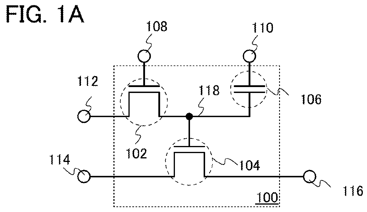
[0062]In the memory element 100 and the memory element 150 described in Embodiment 1 and the memory element 200 described in Embodiment 2, it is necessary to make a potential difference between at least two terminals (precharge operation) before data is read out. For example, in the memory element 100 in FIG. 1A, the fourth terminal 114 and the fifth terminal 116 need to have potentials different from each other.

[0063]Next, description is made on an example of the configuration of the memory element that can be used for the semiconductor device of one embodiment of the present invention, in which precharge operation is unnecessary (see FIGS. 3A and 3B).

[0064]FIG. 3A illustrates an example of the configuration of the memory element that can be used for the semiconductor device of one embodiment of the present invention, in which precharge operation is unnecessary. A memory element 300 illustrated in FIG. 3A includes a first transistor 302, a second transistor 304, a thi...


PUM


Abstract

An error of stored data is detected with high accuracy. Data (e.g., a remainder in a CRC) used for detecting an error is stored in a memory in which an error is unlikely to occur. Specifically, the following semiconductor device is used: a memory element including a plurality of transistors, a capacitor, and a data storage portion is provided in a matrix; the data storage portion includes one of a source and a drain of one of the plurality of transistors, a gate of another one of the plurality of transistors, and one electrode of the capacitor; a semiconductor layer including a channel of the transistor, the one of the source and the drain of which is connected to the data storage portion, has a band gap of 2.8 eV or more, or 3.2 eV or more; and the data storage portion stores data for detecting an error.

Description

BACKGROUND OF THE INVENTION[0001]1. Field of the Invention[0002]The present invention relates to a semiconductor device. In this specification, the semiconductor device refers to a semiconductor element itself or a device including the semiconductor element, and an example of such a semiconductor element is a thin film transistor. Therefore, a liquid crystal display device, a memory device, and the like are also included in the category of the semiconductor device.[0003]2. Description of the Related Art[0004]A programmable semiconductor device is a kind of semiconductor device. The programmable semiconductor device includes a logic circuit which can be reconfigured by a user, and such a semiconductor device is called, for example, a programmable logic device (PLD).[0005]An example of PLD is a semiconductor device having the following structure: a plurality of logic circuits are provided, and a connection between the logic circuits or the function of the logic circuits can be changed...

Claims


Application Information

Patent Timeline
Patent Type & Authority Patents(United States)
IPC IPC(8): G11C29/12G11C11/405G11C29/52G11C29/04G06F11/10G11C16/04
CPCG11C29/04G06F11/1004G11C11/405G11C29/52G11C16/045G11C16/0416G11C16/0433G11C2029/0409G11C2029/0411H01L27/1225G06F3/0619G06F3/064G06F3/0679
Inventor TAKEMURA, YASUHIKO
Owner SEMICON ENERGY LAB CO LTD
Why Eureka
Try Eureka