Electronic device and manufacturing method thereof, electronic apparatus, and moving body

a manufacturing method and electronic device technology, applied in the direction of hermetically sealed casings, semiconductor/solid-state device details, instruments, etc., can solve the problems of reduced air tightness of the cavity, unstable first bonding state, and disadvantages of electronic devices, so as to improve reliability

Active Publication Date: 2016-01-26
SEIKO EPSON CORP
View PDF6 Cites 5 Cited by
  • Summary
  • Abstract
  • Description
  • Claims
  • Application Information

AI Technical Summary

Benefits of technology

[0007]An advantage of some aspects of the invention is to provide an electronic device having improved reliability. Another advantage of some aspects of the invention is to provide a manufacturing method of the electronic device. Still another advantage of some aspects of the invention is to provide an electronic apparatus and a moving body which include the electronic device.
[0011]According to the electronic device according to the application example, the first cavity and the second cavity are isolated from each other by the partition wall portion which is integrally provided in the cover body or the substrate. According to this, the first cavity and the second cavity are configured by only two members of the substrate and the cover body without a seal member. In other words, the bond interface between members, which is required for configuring two cavities in the same package, includes only the bond surface between the substrate and the cover body. Therefore, compared to an electronic device in which a partition wall member other than the substrate and the cover body isolates between the cavities having inner pressures different from each other, an electronic device having improved reliability can be provided.Application Example 2
[0024]According to the manufacturing method of the electronic device of this application example, the sealing of the cavity with which the through-hole does not communicate can be performed in the placing and the accommodating. According to this, the material costs of the seal member which is formed of alloy such as AuGe are reduced, and the sealing process of the through-hole, which requires a temperature control having high accuracy, can be simplified. Therefore, the manufacturing method of the electronic device, which can contribute to reduction of the production costs and simplification of the production processes, can be provided.

Problems solved by technology

On the other hand, since gas viscosity becomes a cause which damps vibration when air (or other gas and the like) exists, the angular velocity sensor is sealed at a decompression atmosphere such as a vacuum atmosphere.
According to this, since cavities, in which the inner pressures are different from each other in the same package, are formed, when bonding reliability between members is decreased, airtightness of the cavities is decreased, and disadvantages occur in the electronic device.
In this case, since the plurality of bonded portions exist, if a second bonding is performed after a first bonding is performed, there is a concern that the first bonding state may be unstable, and it is difficult to secure bonding reliability between each member.
In an electronic device in which cavities having inner pressures different from each other are formed in the same package, when airtightness of the cavities is decreased, defects occur in the function elements accommodated in the cavities, and there is a concern that reliability of the electronic device itself may be decreased.

Method used


Image

  • Electronic device and manufacturing method thereof, electronic apparatus, and moving body
  • Electronic device and manufacturing method thereof, electronic apparatus, and moving body
  • Electronic device and manufacturing method thereof, electronic apparatus, and moving body

Examples


first embodiment

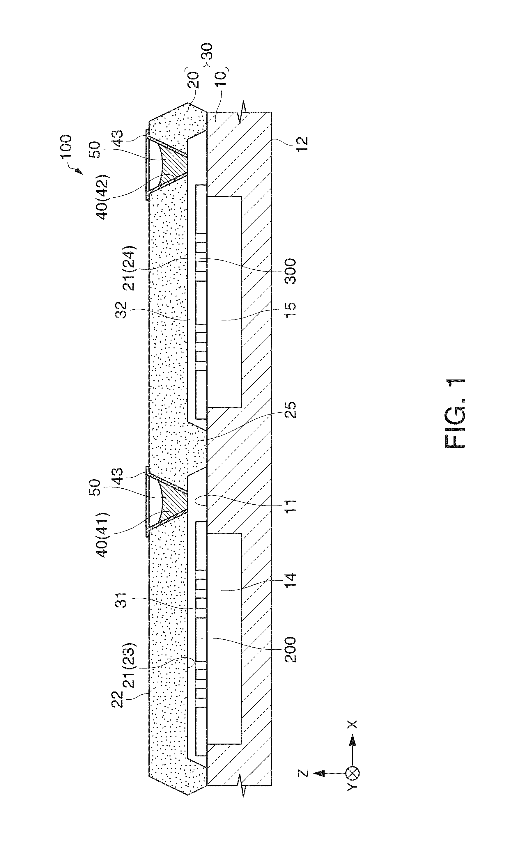
[0055]First, an electronic device according to a first embodiment will be described with reference the drawings. FIG. 1 is a cross-sectional view schematically showing an electronic device 100 according to the first embodiment. For convenience, in the drawings, an X axis, a Y axis, and a Z axis are shown as three axes perpendicular to one another.

[0056]As shown in FIG. 1, the electronic device 100 includes a package 30 which has a substrate 10 and a cover body 20, a through-hole 40 (41 and 42) which is provided in the package 30, a seal member 50 which seals the through-hole 40, and a first and second function elements 200 and 300 which are accommodated in the package 30. Moreover, for convenience, in FIG. 1, the first and second function elements 200 and 300 are shown so as to be simplified.

[0057]The first and second function elements 200 and 300, which are accommodated in the electronic device 100, are sensor elements which detect physical quantities different from each other resp...

second embodiment

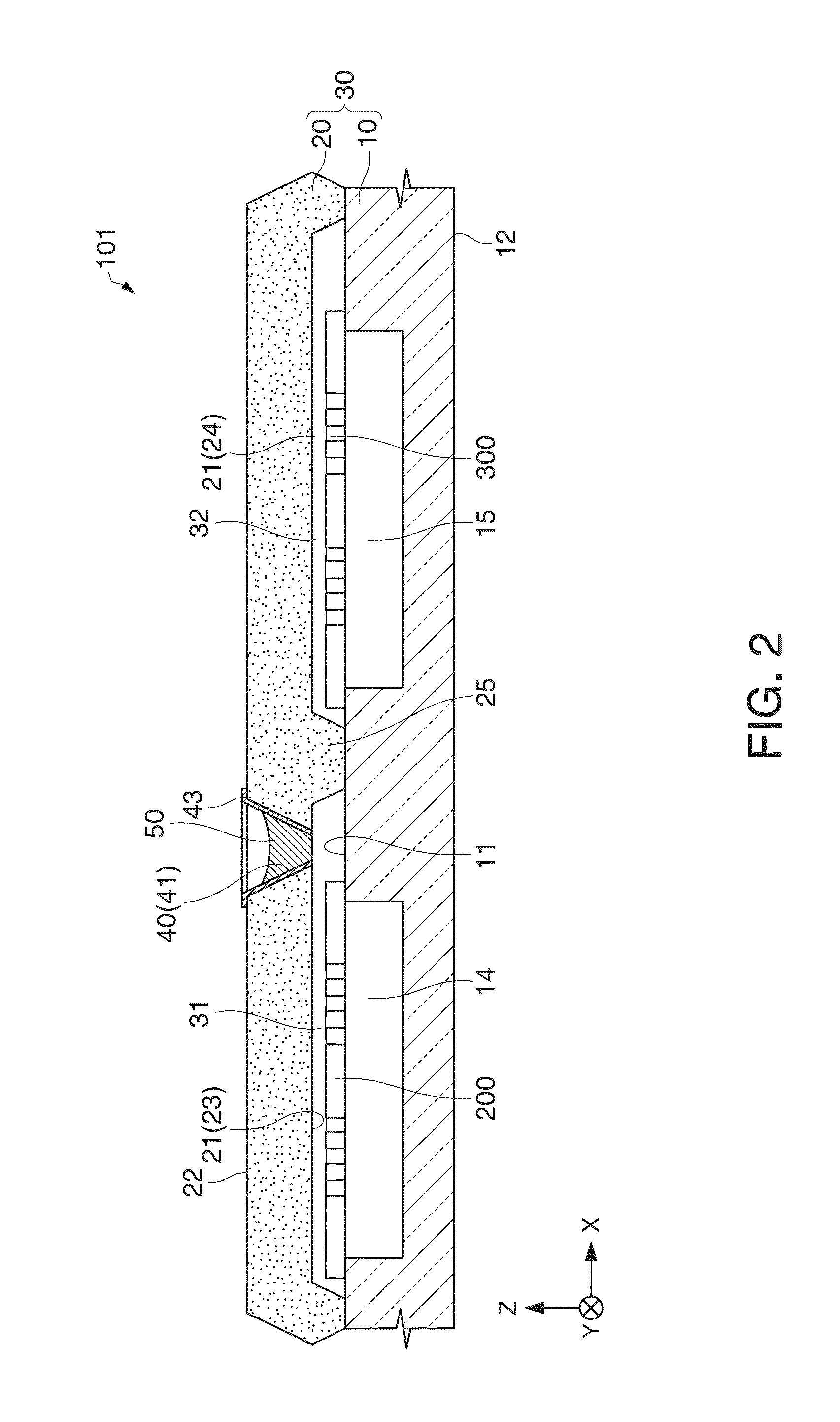
[0075]Next, an electronic device according to a second embodiment will be described with reference to the drawings. FIGS. 2 and 3 are cross-sectional views schematically showing electronic devices 101 and 102 according to the second embodiment. The electronic devices 101 and 102 according to the second embodiment are different from the electronic device 100 according to the first embodiment only in the configuration of the through-hole 40 (first through-hole 41 and second through-hole 42). In descriptions below, only matters in which the electronic devices 101 and 102 according to the second embodiment are different from the device 100 according to the first embodiment will be described. The same reference numerals are attached to the configurations which are previously described, and the detailed descriptions are omitted.

[0076]In the second embodiment, any one of the first through-hole 41 and the second through-hole 42 is provided. Accordingly, in the second embodiment, the through...

modification example

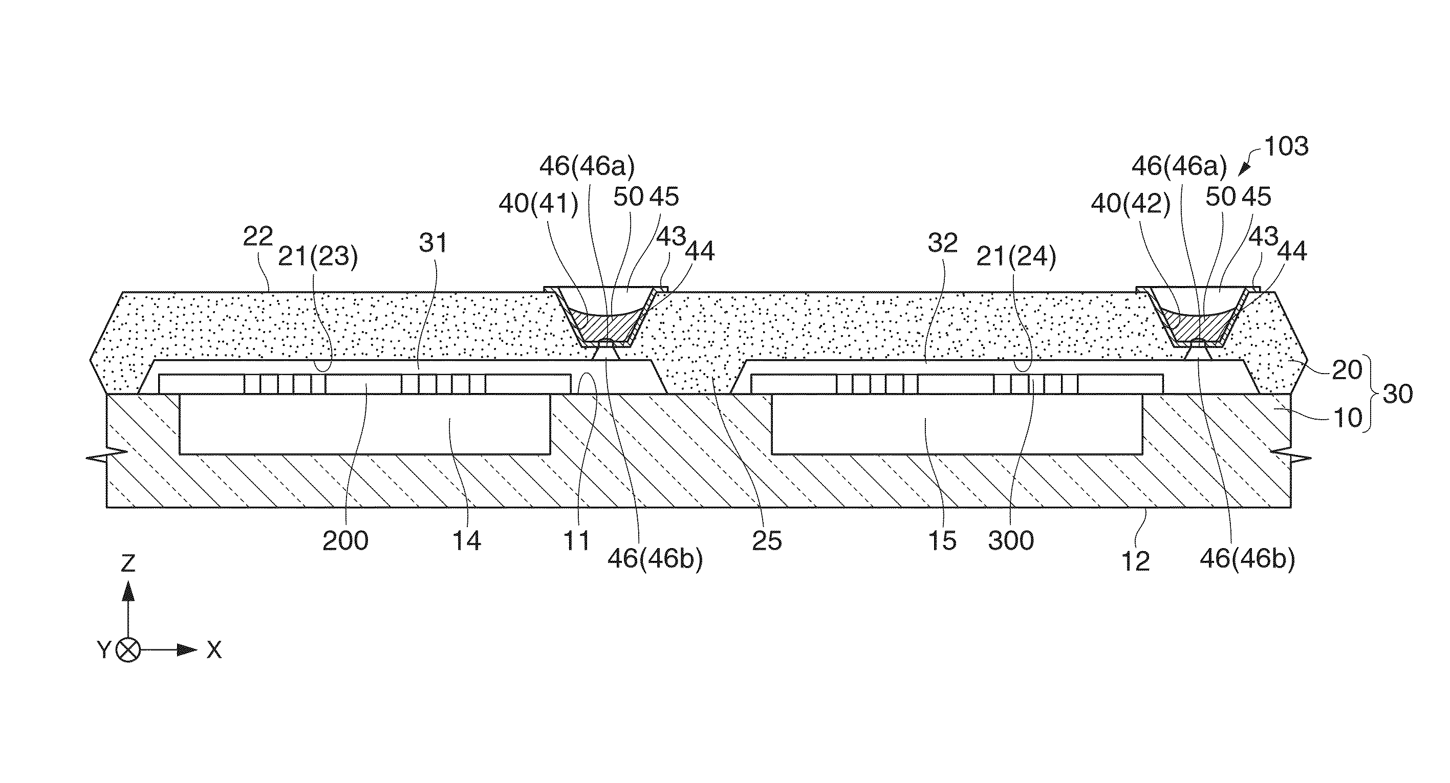
[0087]Next, Modification Example of the electronic device according to the first and second embodiments will be described with reference to drawings. FIG. 4 is a cross-sectional view schematically showing an electronic device 103 according to the Modification Example. The electronic device 103 according to the Modification Example is different from the electronic devices according to the first and second embodiments only in the configuration of the through-hole 40 (first through-hole 41 and second through-hole 42). In descriptions below, only matters which are different from the devices according to the first and second embodiments will be described. The same reference numerals are attached to the configurations which are previously described, and the detailed descriptions are omitted.

[0088]In the electronic device 103 according to the Modification Example, the through-hole 40 includes a bottom surface 44 and communicates with the cavity through a communication hole 46 provided on t...


PUM

PropertyMeasurementUnit
thicknessaaaaaaaaaa
temperatureaaaaaaaaaa

Abstract

An electronic device includes a substrate, a cover body which is placed on the substrate, a first cavity which is surrounded by the substrate and the cover body, and a second cavity which is surrounded by the substrate and the cover body, wherein an inner portion of the first cavity is sealed in a first air pressure atmosphere, and an inner portion of the second cavity is sealed in a second air pressure atmosphere which has a difference of air pressure with respect to the first air pressure atmosphere, a first through-hole, which communicates with the first cavity and is blocked by a seal member, is provided in at least one of the substrate and the cover body, and the first cavity and the second cavity are isolated from each other by a partition wall portion which is integrally provided to the cover body or the substrate.

Description

BACKGROUND[0001]1. Technical Field[0002]The present invention relates to an electronic device and a manufacturing method thereof, an electronic apparatus, and a moving body.[0003]2. Related Art[0004]Recently, for example, an electronic device such as an inertial sensor, which detects physical quantity using technology of silicon Micro Electro Mechanical System (MEMS), has been developed. In JP-A-2002-5950, for example, an electronic device (combined sensor element) which includes an angular velocity sensor and an acceleration sensor is disclosed. For example, the above-described electronic device is used for a camera shake correction function of a digital still camera (DSC), a navigation system of an automobile, an operation input device at a game machine, or the like.[0005]In this way, according to the electronic device in which a plurality of physical quantity detection sensors are mounted into the same package (the same substrate), it is possible to meet demands for size reductio...

Claims


Application Information

Patent Timeline
Patent Type & Authority Patents(United States)
IPC IPC(8): G01C19/56G01P15/125G01C19/5747B81B7/00H05K13/00G01C19/5719H05K5/06G01P1/02B81B7/02G01P15/097
CPCH05K5/069B81B7/0041B81B7/02G01C19/5719G01C19/5747G01P15/097G01P15/125H05K13/00B81C2203/0145Y10T29/49002
Inventor TAKIZAWA, TERUO
Owner SEIKO EPSON CORP
Why Eureka
Try Eureka