

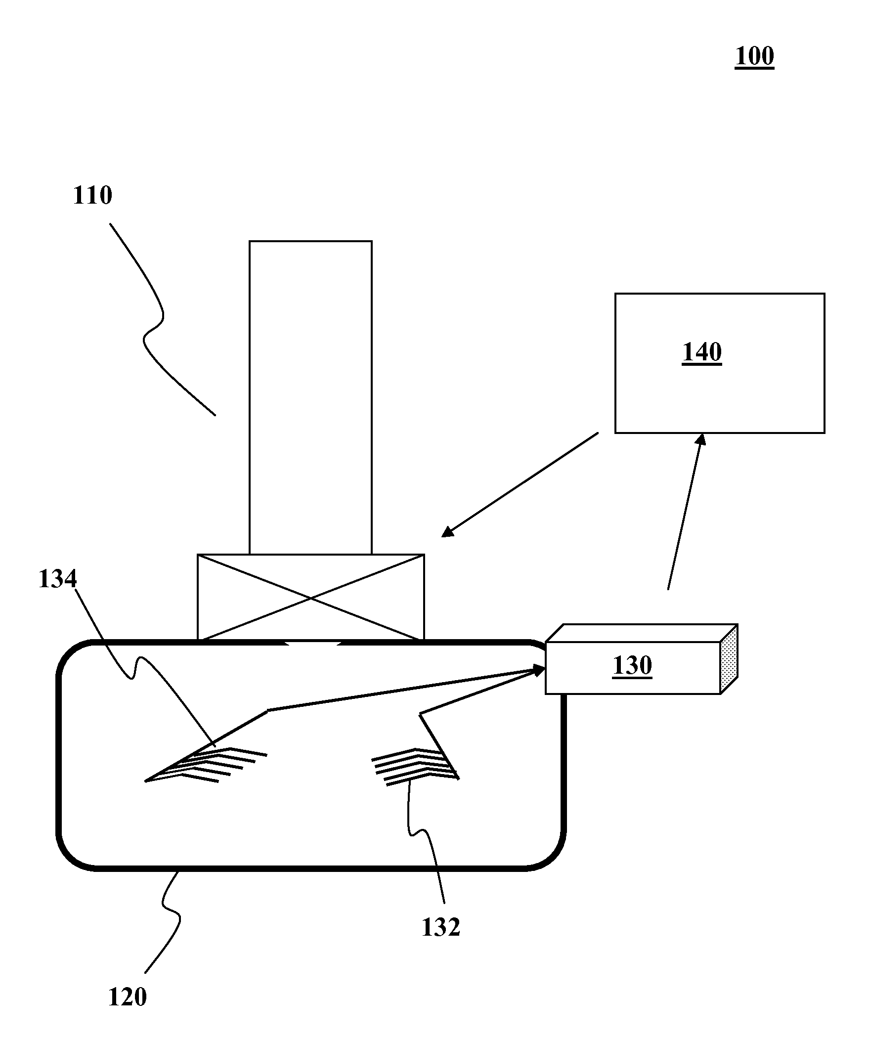
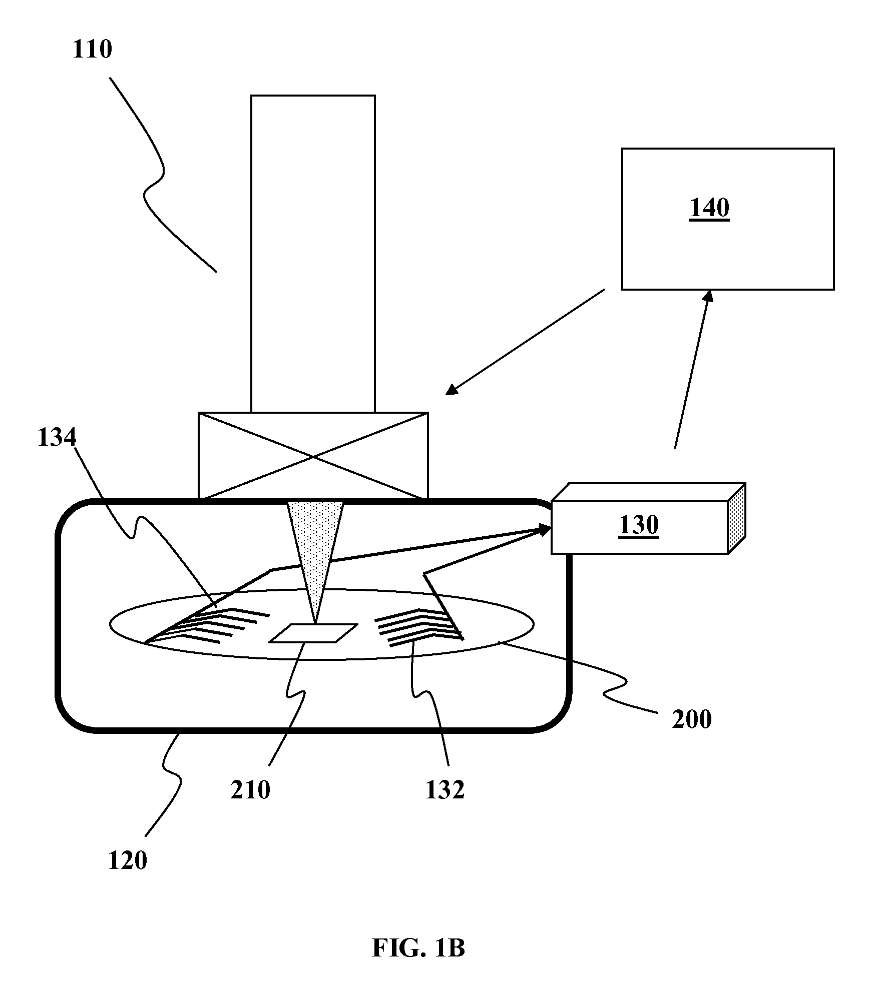
Defect inspection apparatus, system, and method
a technology of defect inspection and inspection apparatus, applied in the field of specimen inspection, can solve the problems of difficult to detect defects using optical methods, severely hampered signal to noise, and high cost, and achieve the effect of efficient and effective testing of defects
- Summary
- Abstract
- Description
- Claims
- Application Information
AI Technical Summary
Benefits of technology
Problems solved by technology
Method used
Image

Examples
Embodiment Construction
[0020]Although the following detailed description contains many specific details for the purposes of illustration, anyone of ordinary skill in the art will appreciate that many variations and alterations to the following details are within the scope of the invention. Accordingly, the exemplary embodiments of the invention described below are set forth without any loss of generality to, and without imposing limitations upon, the claimed invention. Additionally, because components of embodiments of the present invention can be positioned in a number of different orientations, the directional terminology is used for purposes of illustration and is in no way limiting. It is to be understood that other embodiments may be utilized and structural or logical changes may be made without departing from the scope of the present invention.
[0021]In this document, the terms “a” and “an” are used, as is common in patent documents, to include one or more than one. In this document, the term “or” is...
PUM
 Abstract
Description
Claims
Application Information