Substrate-free mechanical interconnection of electronic sub-systems using a spring configuration

a technology of mechanical interconnection and electronic sub-system, which is applied in the direction of multiple connection sub-assemblies, electrical devices, waveguides, etc., can solve the problems of less straightforward systems, similar but larger volume, and the desktop computer industry, so as to eliminate the intended functions of the system and eliminate unnecessary impediments to access

Active Publication Date: 2016-04-05
CUBIC CORPORATION
View PDF218 Cites 35 Cited by
  • Summary
  • Abstract
  • Description
  • Claims
  • Application Information

AI Technical Summary

Benefits of technology

[0018]A beneficial aspect of structural systems in accordance with the present invention is that the majority of unnecessary material or substances which do not add value to, or may even detract from, the intended functions for the system can be eliminated. Thus, mass, bulk, physical properties mismatch (such as expansion coefficient mismatch) of the substrate may be eliminated by eliminating the substrate, thereby eliminating unnecessary impediments to access to various surfaces of the system or subsystem.

Problems solved by technology

In building complex multilayer electronic and electro-mechanical systems, particularly those of high complexity, and high value, there remain challenges in building said systems with sufficiently high yield and or low re-work to produce said systems economically.
For example, the desktop computer industry approached a similar but larger volume problem since at least the 1980s by creating motherboards and computer daughter cards with standardized connectors where the card and motherboard could be electrically and mechanically joined by one plugging into arrayed connectors and then being mechanically fastened to a metal chassis, for example, by screws.
This problem however is less straightforward for systems where one or more of the size, complexity, integration, weight, performance, or cost of desired interconnection becomes a limiting factor to produce the desired system.
Even cooling such systems, for example in the aforementioned desktop computer, can remain a challenge, since forced air by using multiple fans becomes a difficult method to remove heat from all locations necessary.
Also, thermal conduction through heat pipes and thermal busses and ground planes make modularity a challenge.
This trend of pushing so much desired functionality into densely integrated chips which are permanently attached, combined with a rapid obsolescence rate has made it almost commonplace to dispose of the system if it fails; repair is too complicated and / or the cost of such repair exceeds the value of the system.
Compare this situation to one where the value of the components or chips or modules are very high but one or more of the integration density, size, weight, yield, performance and price are limiting factors, such that rework and modularity are required.
Add to this the inability for any single semiconductor technology to provide all the performance or functions desired, or there simply being added constraints that make it impractical to integrate all the functions intimately into a chip or wafer level process.
The area it needs to consume is based on performance limitations of its transmit / receive elements, but are also limited by the frequencies / wavelengths of its operation.
However solving the challenges of modularity and rework when size and performance and even mechanical requirements of the necessary interconnect remains unsolved.
Currently the microelectronics industry approaches similar commercial problems using methods such as chip-stacking technology, through-substrate vias, tiered wirebonds, and in some cases attempts to integrate more than one semiconductor technology onto a single wafer.
While these approaches may solve certain problems in volume production for reduced size, weight, and interconnection, they are not technologies that readily lend themselves to lower volumes, particularly where it is desired to have relatively un-compromised performance, rework, or modularity.
A further problem in existing electronic and electromechanical systems relates to chip or component interconnects.
Independently fabricated and integrated connectors have the disadvantage of consuming substantial volume, size and even weight compared to the dimensions of chips and PolyStrata® integration substrates.
In addition when many such interconnections are needed, substantial joining force and size mismatch become a limiting factor, for example in connecting dozens or hundreds of RF and DC interconnects.
As frequency scales to mm-wave and beyond, loss and mismatch also become greater problems.
Those interconnections based on solder joints have the disadvantage of often requiring the reflow of the solder to ensure a stable DC and RF junction that for example can allow testing or use in the field.
Such reflow on a small scale becomes a challenge as, in increasingly small areas, limiting the flow or wicking or capillary action of the solder—as well as maintaining a thermal solder reflow or bonding hierarchy that doesn't interfere with the attach of nearby chips or other components or modules—becomes difficult to manage.
Also solders in substantially small volumes become difficult to control compositionally due to mechanisms such as interdiffusion and consumption of noble metals and diffusion barriers that may be applied in the junction regions.
Embrittlement of the joint are common issues that arise when small solder volumes are utilized.

Method used


Image

  • Substrate-free mechanical interconnection of electronic sub-systems using a spring configuration
  • Substrate-free mechanical interconnection of electronic sub-systems using a spring configuration
  • Substrate-free mechanical interconnection of electronic sub-systems using a spring configuration

Examples


Embodiment Construction

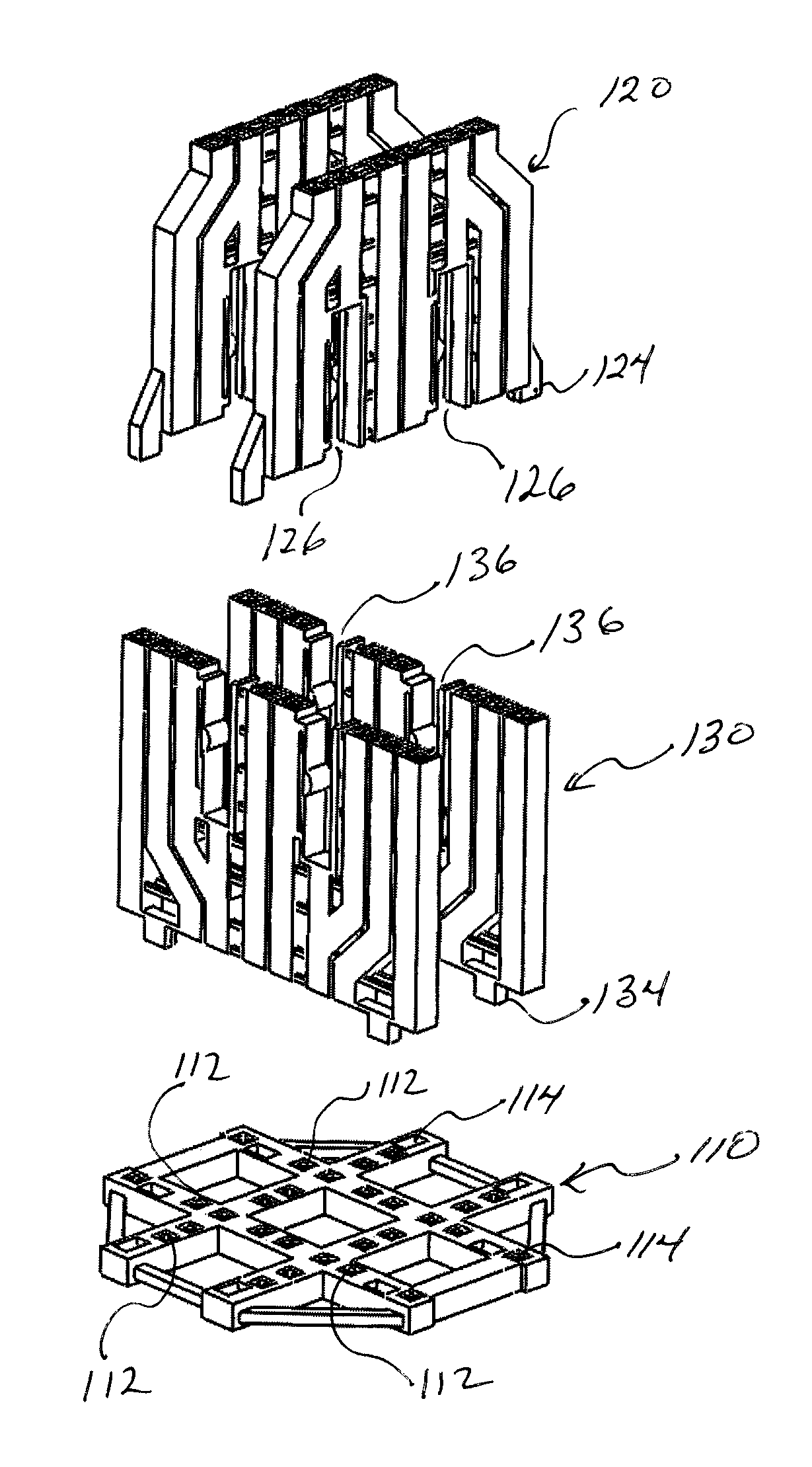
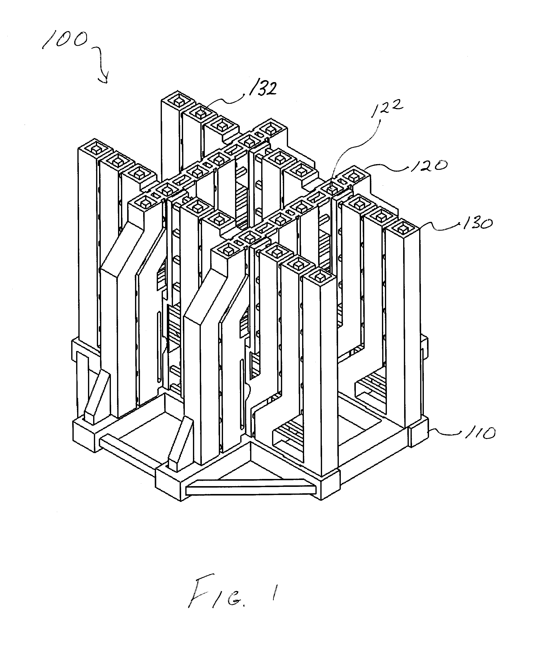
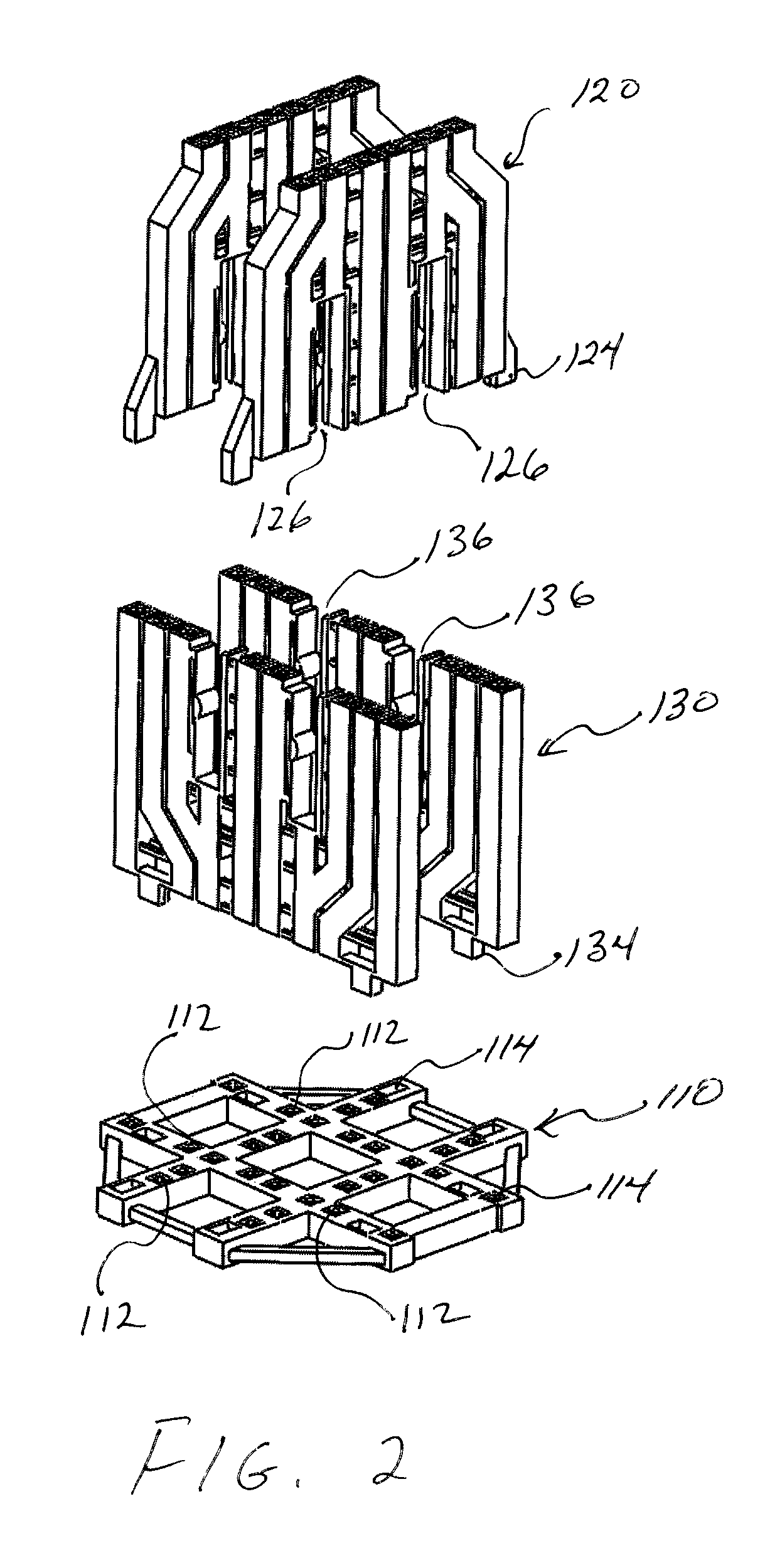
[0040]Referring now to the figures, wherein like elements are numbered alike throughout, FIGS. 1 and 2 schematically illustrate isometric views of an exemplary substrate-free, interconnected electronic mechanical structural system 100 (FIG. 1) in accordance with the present invention, in both assembled and exploded views, respectively. The interconnected electronic mechanical structural system 100 may include first and second substrate-free, electronic subsystems 120, 130 and a substrate-free, electronic base plate 110 each of which may include electronic components, such as coaxial waveguides 112 (FIG. 2), 122 (FIG. 1), 132, (FIG. 1) as well as mechanical connection features, such as complementary mating slots 126, 136, and mounting pegs 124, 134 with complementary mounting holes 114, for example, FIG. 2. The mechanical connection features, e.g., slots 126, 136, pegs 124, 134, justification springs 128 and holes 114, may be configured to permit the substrate-free, electronic subsys...


PUM


Abstract

Substrate-free mechanical structural systems comprised of interconnected subsystems of electronic and/or electromechanical components are provided.

Description

RELATED APPLICATIONS[0001]This application claims the benefit of priority of U.S. Provisional Application No. 61 / 788,675, filed on Mar. 15, 2013, the entire contents of which application(s) are incorporated herein by reference.FIELD OF THE INVENTION[0002]The present invention relates generally to substrate-free, interconnected electronic and / or electromechanical systems, and more particularly, but not exclusively, to substrate-free mechanical structural systems comprised of interconnected subsystems of electronic and / or electromechanical components.BACKGROUND OF THE INVENTION[0003]There exists a need to create electronic and electromechanical systems often comprising dozens to many thousands of interconnects between subassemblies or modules. Several to many of said subassemblies may require to be joined to provide a solution for the final assembly that includes electrical, thermal, optical, mechanical and other forms of transduction and communication and also provide stability and s...

Claims


Application Information

Patent Timeline
Patent Type & Authority Patents(United States)
IPC IPC(8): H01P1/04H05K7/02H01P3/06H01P11/00H05K13/00
CPCH01P3/06H05K7/026H01P11/001H05K13/0023H01P1/045H01P5/12H05K7/005H05K7/02
Inventor HOVEY, IANREID, J. ROBERTSHERRER, DAVIDSTACY, WILLVANHILLE, KEN
Owner CUBIC CORPORATION
Why Eureka
Try Eureka