Light-emitting device and electronic device using light-emitting device
a technology of light-emitting devices and electronic devices, applied in the direction of solid-state devices, electric lighting sources, electric lighting sources, etc., can solve the problems of light-emitting elements being damaged and separated, and achieve the effect of high reliability and preventing damag
- Summary
- Abstract
- Description
- Claims
- Application Information
AI Technical Summary
Benefits of technology
Problems solved by technology
Method used
Image
Examples
embodiment 1
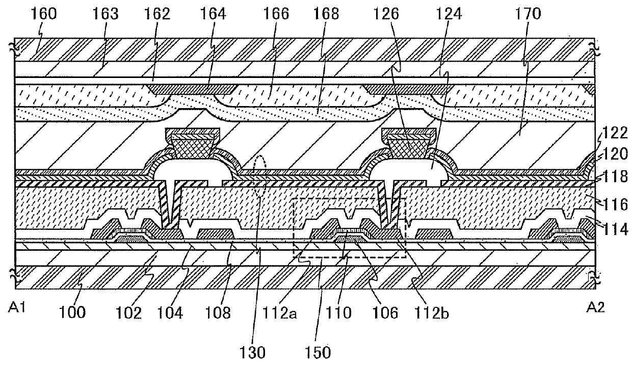
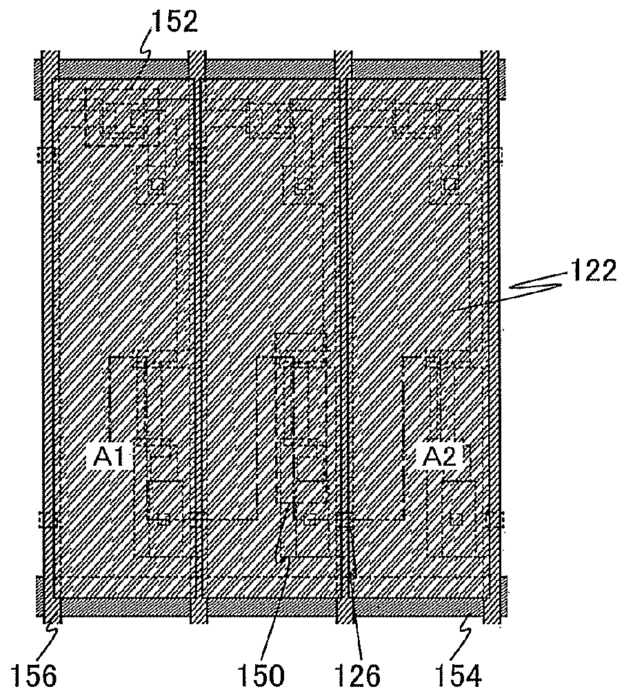
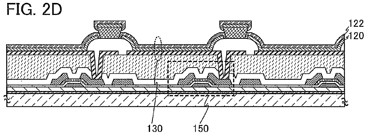
[0039]In this embodiment, according to one embodiment of a light-emitting device of the present invention, a structure of the light-emitting device is described with reference to FIGS. 1A and 1B, and then a method for manufacturing the light-emitting device is described with reference to FIGS. 2A to 2D, FIGS. 3A to 3C, FIGS. 4A and 4B, and FIGS. 5A and 5B.
Structure of Light-Emitting Device
[0040]FIG. 1A is a top view of a first substrate 100 seen from a second electrode layer 122 side, which illustrates a part of a pixel of the light-emitting device. FIG. 1B is a cross-sectional view taken along broken line A1-A2 in FIG. 1A. In the top view of FIG. 1A, some components (e.g., a partition wall 124, and the like) of the present invention are omitted in order to avoid complex views.
[0041]In the light-emitting device shown in FIG. 1A, a plurality of source wirings 156 is provided parallel to (extending in the vertical direction in the drawing) and apart from each other, and a plurality of...
embodiment 2
[0130]A structure body used for a light-emitting device of the present invention, which has a different structure from the structure body 126 described in Embodiment 1, will be described with reference to FIGS. 6A to 6D.
[0131]Note that the same reference numerals are used for the same parts as those of the light-emitting device in Embodiment 1, and description of the parts with the same reference numerals will be omitted here.
[0132]The light-emitting device shown in FIG. 6A has a structure body 206 including a first structure body 202 and a second structure body 204 over the partition wall 124.
[0133]As a method for forming the structure body 206, a film formed of an organic insulating material is formed; then, a film formed of an inorganic insulating material is formed thereover. After that patterning is performed on a desired region, the film formed of the inorganic insulating material is processed, and then the film formed of the organic insulating material is processed using the ...
embodiment 3
[0153]In this embodiment, description is made on the arrangement of pixels of light-emitting devices in which the structure body 126 described in Embodiment 1 and the structure bodies 206, 208, 210, and 214 described in Embodiment 2 are used with reference to FIGS. 7A to 7D.
[0154]FIGS. 7A to 7D are top views of part of pixels of the light-emitting device. In this embodiment, the position of the structure body in each pixel is described; thus, some components (for example, the transistor 150, the light-emitting element 130, and the like) of the present invention are omitted in order to avoid complex views each of the light-emitting devices shown in FIGS. 7A to 7D, a plurality of source wirings 156 is provided parallel to (extending in the vertical direction in the drawing) and apart from each other, and a plurality of gate wirings 154 is provided parallel to (extending in the horizontal direction in the drawing) and apart from each other. A substantially rectangular region is surroun...
PUM
 Abstract
Description
Claims
Application Information


