Method for producing a leadthrough for an optical conductor
a leadthrough and optical conductor technology, applied in the direction of optics, instruments, optical light guides, etc., can solve the problems of increased material costs, inability to produce by injection moulding process, and increased space requirements for components, so as to simplify the subsequent bending of the tube and simplify the threading of the optical waveguide into the tube
- Summary
- Abstract
- Description
- Claims
- Application Information
AI Technical Summary
Benefits of technology
Problems solved by technology
Method used
Image
Examples
first embodiment
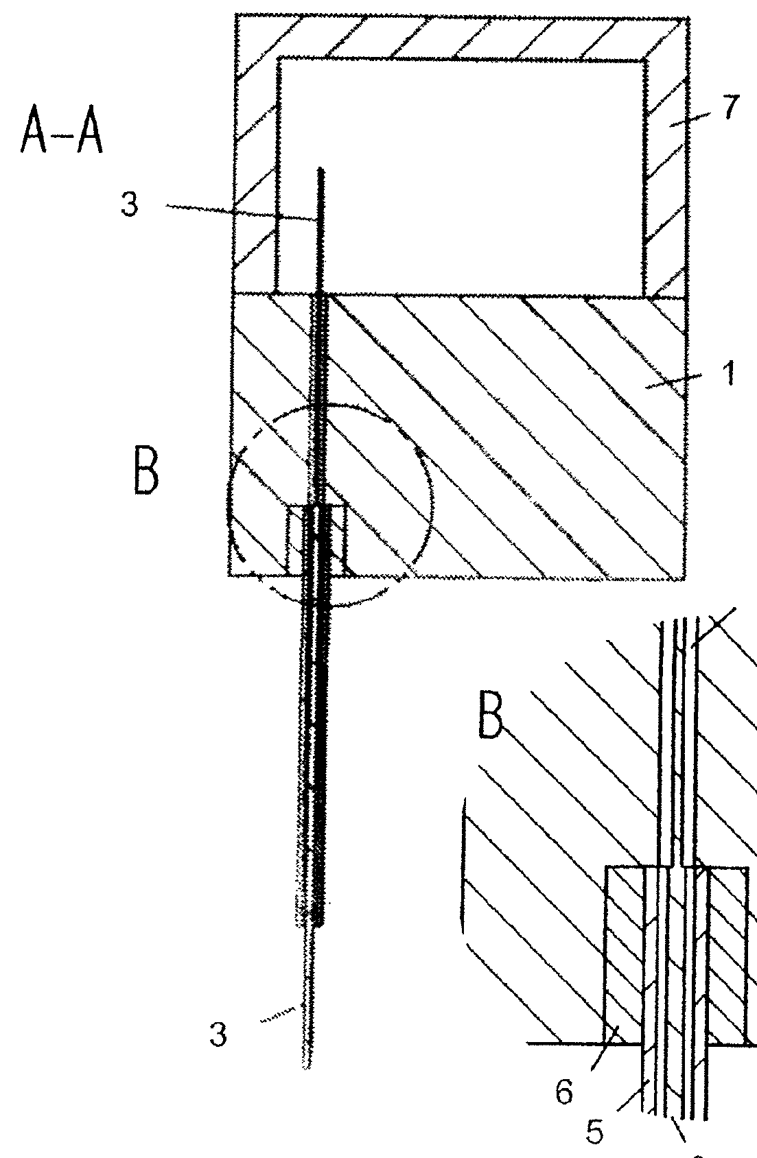
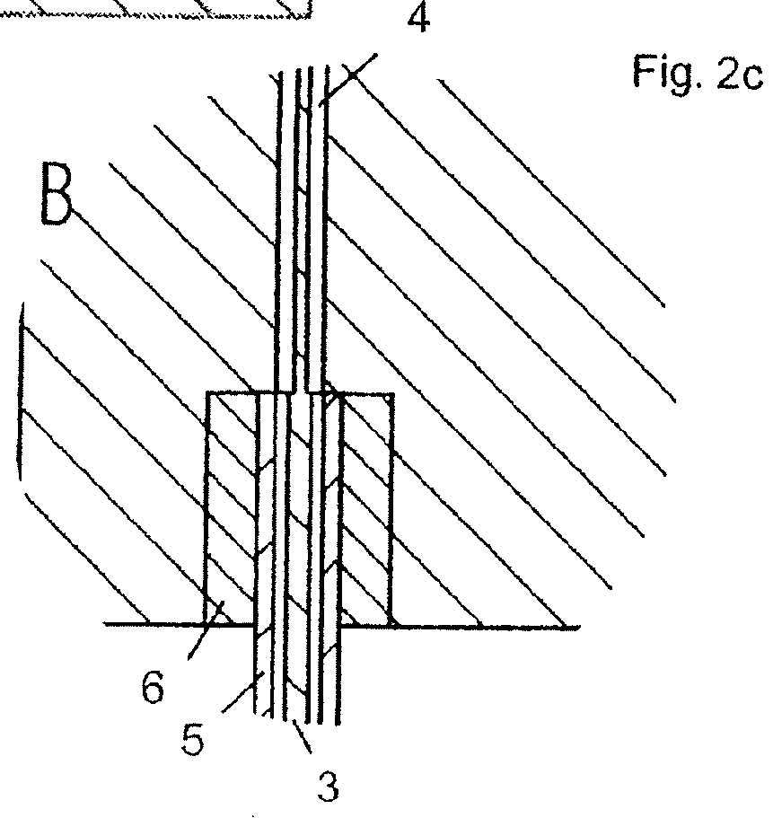
[0044]the present invention is shown in FIGS. 3a to 3c. FIG. 3a shows a top view of a suitable housing. FIG. 3b shows a sectional view along the line A-A of FIG. 3a and FIG. 3c shows a detail enlargement of FIG. 3b.
[0045]Here also, the housing consists of two housing parts 1, 7. One housing part 1 has a stepped passage opening. The passage opening has a section with small diameter and a section with large diameter. The section with small diameter has a small aspect ratio compared with the embodiment of the state of the art shown in FIG. 2.
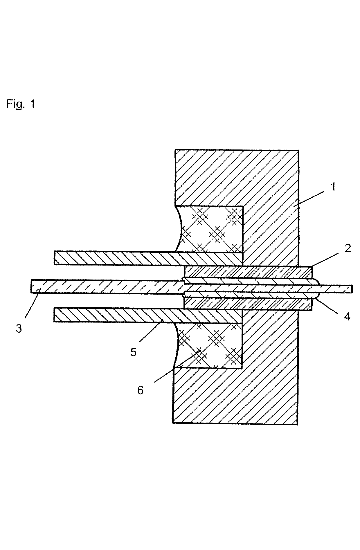
[0046]The small aspect ratio makes it possible to produce housing part 1 by the injection moulding process. In order to obtain a hermetically sealed leadthrough, a metal tube 2 is inserted into the passage opening and sintered together with the housing part 1. The channel with large aspect ratio necessary for the hermetically sealed leadthrough is now no longer provided by the passage opening through the housing part 1, but by the metal tube 2.
[00...
second embodiment
[0049]the invention is shown in FIGS. 4a to 4c. In this embodiment the metal tube 2 is widened or flared at one end. In the same way the mouth region of the passage opening arranged in the housing part 1 is widened, with the result that, as can be seen in particular in FIG. 4c, the widening 8 of the metal tube 2 can be fully accommodated inside the housing part 1 and ends flush with the surface.
third embodiment
[0050]As shown in FIGS. 5a to 5c, which represent the invention, it is not essential that the metal tube 2 ends flush with the surface of the housing part 1. Rather, it is equally possible that the metal tube 2 projects beyond the surface of the housing part 1, as can be seen in particular in FIG. 5c. Through this measure the thickness of the housing part 1 can be further reduced or the diffusion length easily increased.
PUM
| Property | Measurement | Unit |
|---|---|---|
| aspect ratio | aaaaa | aaaaa |
| melting point | aaaaa | aaaaa |
| melting point | aaaaa | aaaaa |
Abstract
Description
Claims
Application Information


