
Complementary metal-oxide-semiconductor (CMOS) analog switch circuit

a metal-oxide-semiconductor and analog switch technology, applied in the field of circuit design, can solve the problems of increased conduction resistance, increased threshold voltage in the transistor increases power consumption, and interferes with linear characteristics and harmonic distortion of an analog switch, and achieves the effect of substrate

Active Publication Date: 2016-07-05
MAGNACHIP SEMICONDUCTOR LTD
View PDF30 Cites 0 Cited by
  • Summary
  • Abstract
  • Description
  • Claims
  • Application Information

AI Technical Summary

Benefits of technology

[0047]The CMOS analog switch circuit with the above architecture provides certain effects.
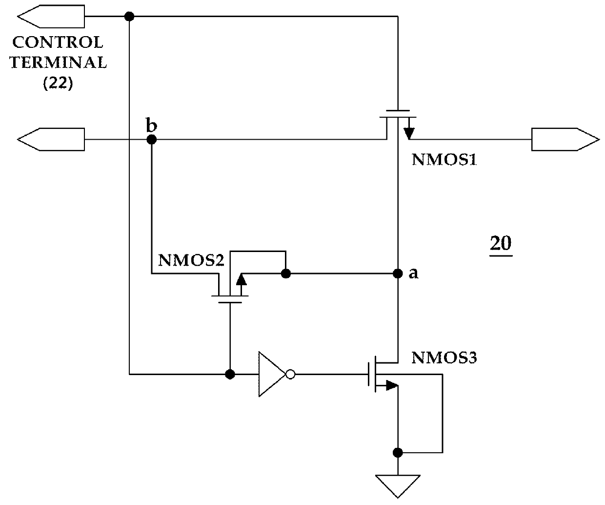
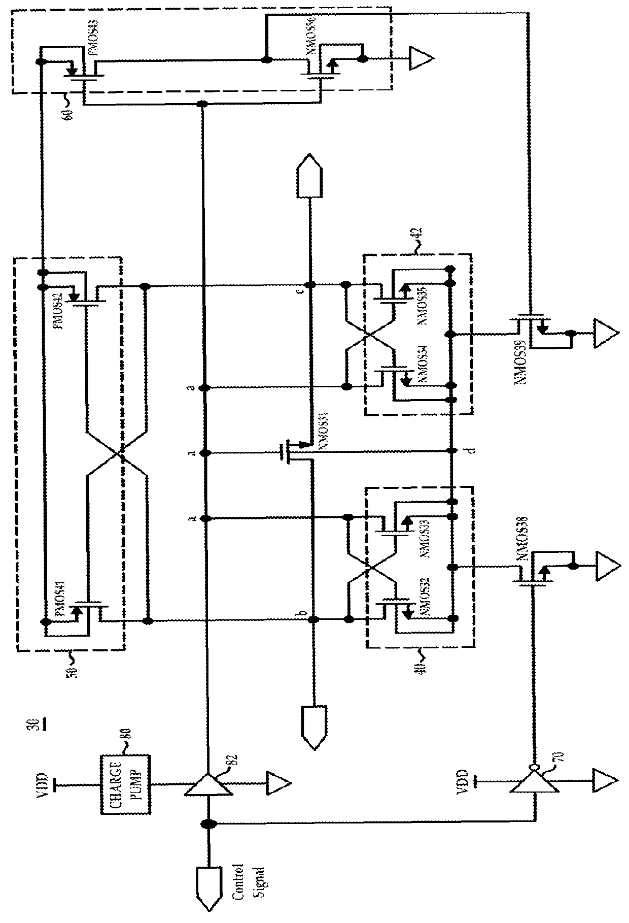
[0048]Since the voltages at both ends of a MOS in a switch-on state are biased to the substrate node of the MOS using a minimum voltage extractor when a supply voltage is applied, the source voltage and the substrate voltage of the MOS are same. As a result, a substrate effect is eliminated.
[0050]According to various examples, the CMOS analog switch has a circuit structure that addresses the issues associated with related switching structures. For example, the substrate effect is eliminated, and the floating of substrate voltage is also eliminated.
[0052]Furthermore, when implemented in sample and hold circuit environment, the CMOS analog switch also improves harmonic distortion. For example, a sample and hold circuit environment includes an analog design that samples the voltage of a continuously varying analog signal and holds its value at a constant level for a specified minimum period of time.

Problems solved by technology

Increased threshold voltage in the transistor increases power consumption.
Furthermore, increased conduction resistance hinders normal on and off switching operation of the transistor.
Furthermore, the substrate effect also interferes with the linear characteristic and the harmonic distortion of an analog switch.
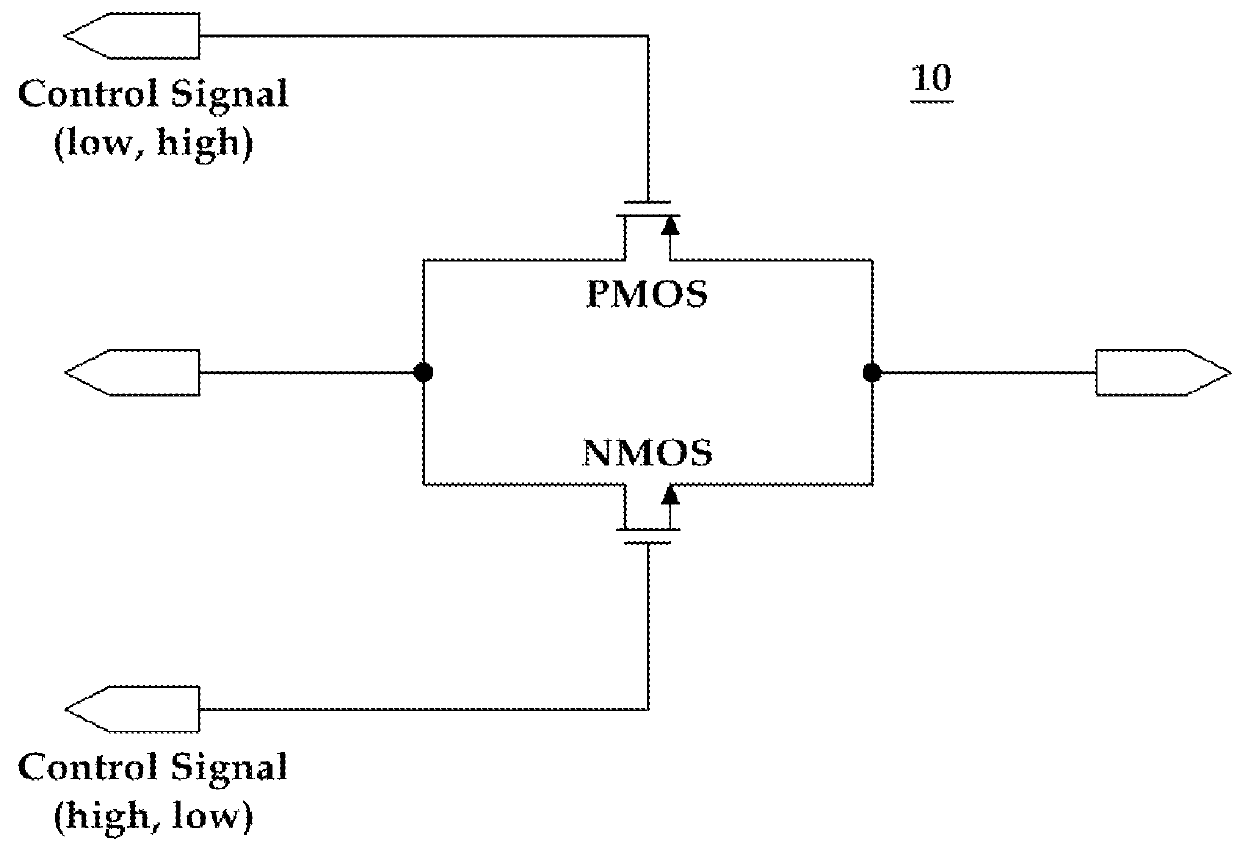
However, the example of FIG. 2 is limited to functioning only in situations when supply voltage (vdd) is successfully fed.
Accordingly, when the supply voltage (vdd) is not successfully applied, other issues with the operation of the switch occur.
In such an unstable state, latch-up and leakage current from the switch may occur.

Method used


Image

  • Complementary metal-oxide-semiconductor (CMOS) analog switch circuit
  • Complementary metal-oxide-semiconductor (CMOS) analog switch circuit
  • Complementary metal-oxide-semiconductor (CMOS) analog switch circuit

Examples


Embodiment Construction

[0059]The following detailed description is provided to assist the reader in gaining a comprehensive understanding of the methods, apparatuses, and / or systems described herein. However, various changes, modifications, and equivalents of the systems, apparatuses and / or methods described herein will be apparent to one of ordinary skill in the art. The progression of processing steps and / or operations described is an example; however, the sequence of and / or operations is not limited to that set forth herein and may be changed as is known in the art, with the exception of steps and / or operations necessarily occurring in a certain order. Also, descriptions of functions and constructions that are well known to one of ordinary skill in the art may be omitted for increased clarity and conciseness.

[0060]The features described herein may be embodied in different forms, and are not to be construed as being limited to the examples described herein. Rather, the examples described herein have bee...


PUM


Abstract

A Complementary Metal-Oxide-Semiconductor (CMOS) analog switch has a circuit structure such that when a supply voltage is applied, the CMOS analog switch biases voltages at both ends of a Metal-Oxide-Semiconductor Field Effect Transistor (MOS) device, which switches on upon application of supply voltage, to a substrate node of MOS, or biases the substrate voltage of MOS device to a ground voltage state during a switching-off operation. The substrate voltage of MOS device in floating state is still biased to the ground voltage state even when abnormal, high voltages are applied to both ends of the MOS device. As a result, threshold voltage and conduction resistance decrease compared to related analog switches, and frequency bandwidth increases.

Description

CROSS-REFERENCE TO RELATED APPLICATIONS[0001]This application claims the benefit under 35 U.S.C. §119(a) of Korean Patent Application No. 10-2013-0079986 filed on Jul. 8, 2013, in the Korean Intellectual Property Office, the entire disclosure of which is incorporated herein by reference for all purposes.BACKGROUND[0002]1. Field[0003]The following description relates to circuit design. Also, the following description relates to circuits that are Complementary Metal-Oxide-Semiconductor (CMOS) switch circuit, and also to a CMOS analog switch circuit configured to suppress substrate effects from generating due to a voltage difference between substrate and source terminals and to maintain substrate (body) voltage to ground voltage (vss) state irrespective of whether supply voltage (vdd) is applied or not. For example, the description includes biasing the substrate voltage of a transistor operating as a switching device.[0004]2. Description of Related Art[0005]Analog switches switch on an...

Claims


Application Information

Patent Timeline
Patent Type & Authority Patents(United States)
IPC IPC(8): G11C27/02H03K17/06H03K17/041G05F3/16
CPCG11C27/02H03K17/04106H03K17/063G05F3/16H03K2217/0018H03K2217/0054H03K17/687
Inventor KWON, BRANDONSUL, JUNG HOON
Owner MAGNACHIP SEMICONDUCTOR LTD
Learn More