

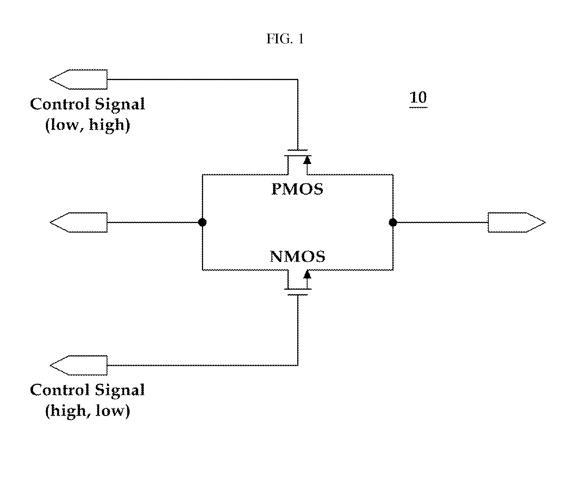
Complementary metal-oxide-semiconductor (CMOS) analog switch circuit
a metal-oxide-semiconductor and analog switch technology, applied in the field of circuit design, can solve the problems of increased conduction resistance, increased threshold voltage in the transistor increases power consumption, and interferes with linear characteristics and harmonic distortion of an analog switch, and achieves the effect of substrate
- Summary
- Abstract
- Description
- Claims
- Application Information
AI Technical Summary
Benefits of technology
Problems solved by technology
Method used
Image

Examples
Embodiment Construction
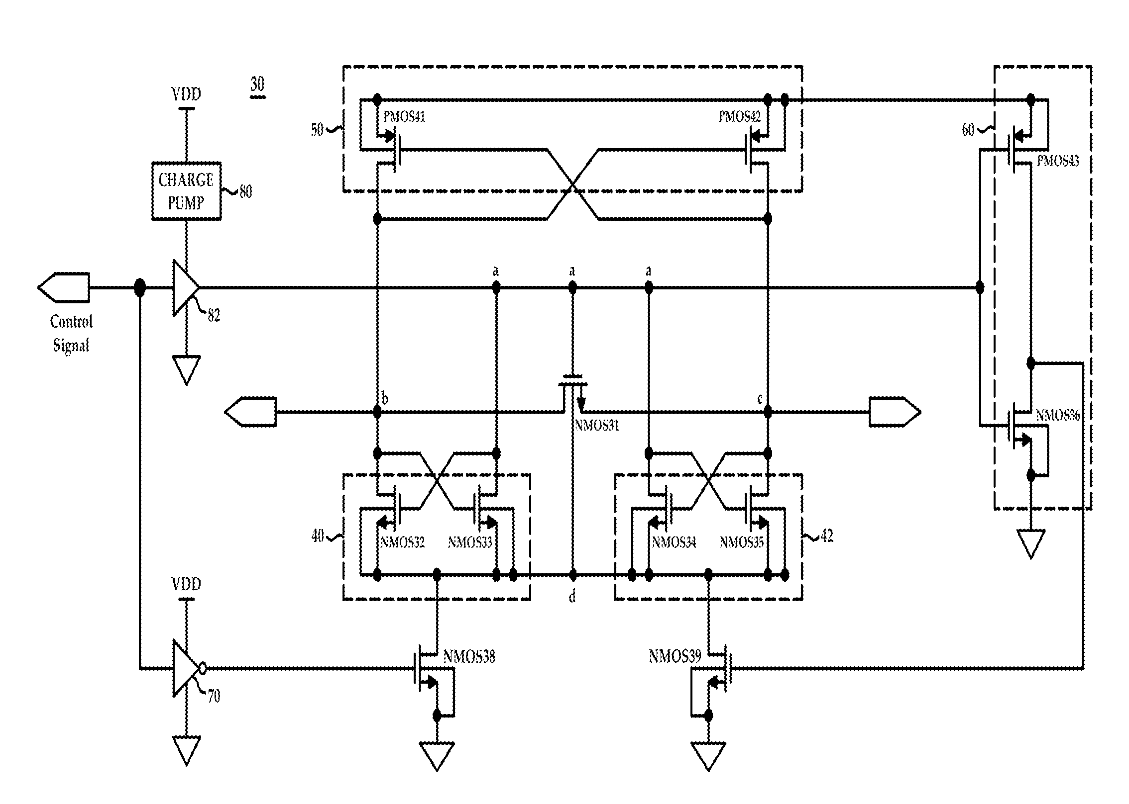
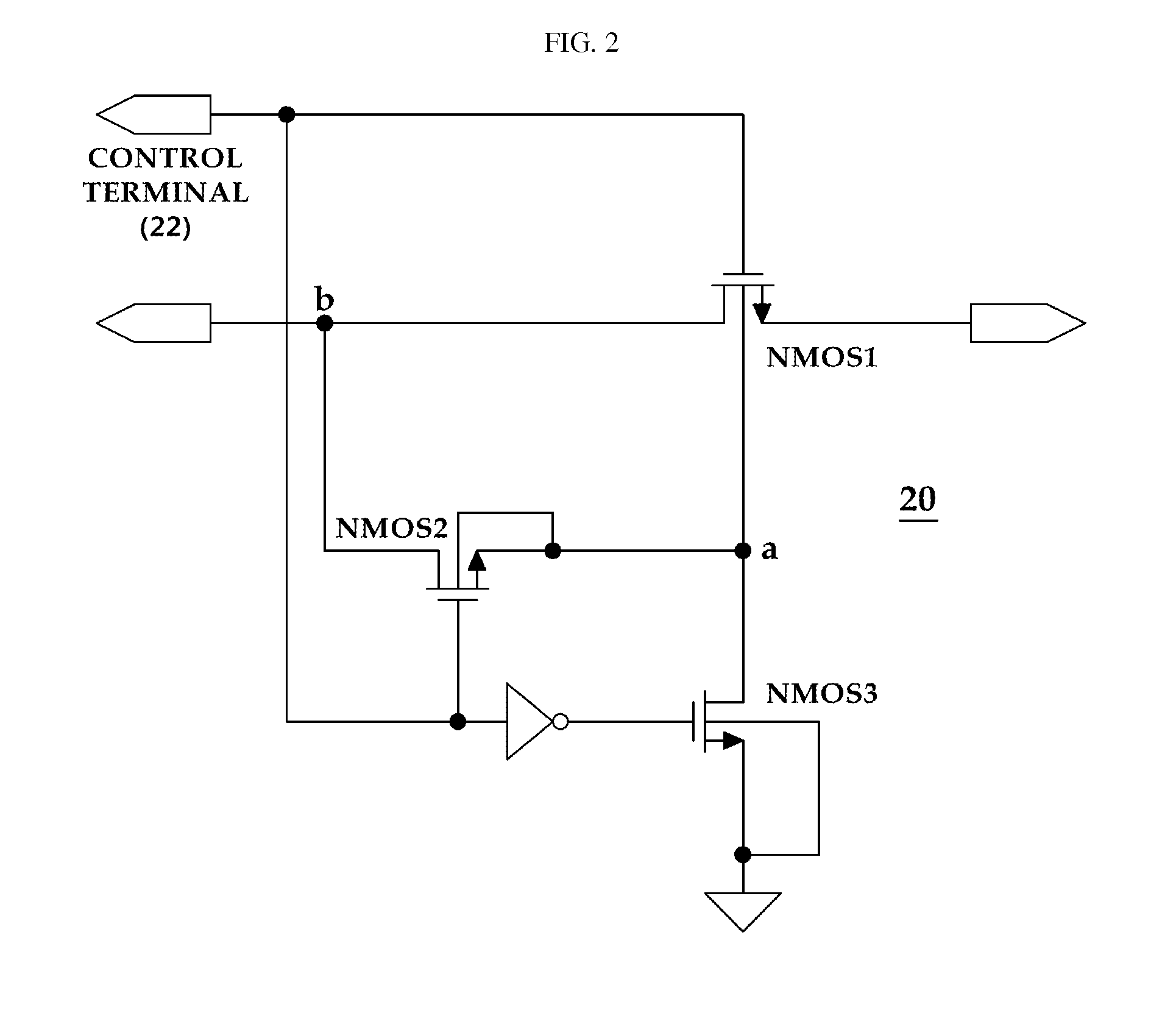
[0059]The following detailed description is provided to assist the reader in gaining a comprehensive understanding of the methods, apparatuses, and / or systems described herein. However, various changes, modifications, and equivalents of the systems, apparatuses and / or methods described herein will be apparent to one of ordinary skill in the art. The progression of processing steps and / or operations described is an example; however, the sequence of and / or operations is not limited to that set forth herein and may be changed as is known in the art, with the exception of steps and / or operations necessarily occurring in a certain order. Also, descriptions of functions and constructions that are well known to one of ordinary skill in the art may be omitted for increased clarity and conciseness.
[0060]The features described herein may be embodied in different forms, and are not to be construed as being limited to the examples described herein. Rather, the examples described herein have bee...
PUM
 Abstract
Description
Claims
Application Information