
Semiconductor device and semiconductor device manufacturing method

a semiconductor device and semiconductor technology, applied in the direction of manufacturing tools, welding/soldering/cutting articles, manufacturing tools, etc., can solve the problems of reducing the reliability of a semiconductor device obtained by using, affecting the application region of solder, and affecting the reliability of a semiconductor device. achieve the effect of preventing the concentration of thermal strain occurring in solder and high reliability

Active Publication Date: 2016-08-16
FUJI ELECTRIC CO LTD
View PDF6 Cites 0 Cited by
  • Summary
  • Abstract
  • Description
  • Claims
  • Application Information

AI Technical Summary

Benefits of technology

[0008]It is desirable that thermal conductivity from the insulating substrate to the radiating member is improved by widening the application region of the solder applied between the insulating substrate and radiating member. However, in the heretofore described technology, the application region of the solder is limited by the pillars disposed on the periphery of the solder. Also, in the heretofore described technology, because the thermal expansion of the pillars is utilized in order to widen the gap between the insulating substrate and radiating member, the insulating substrate and radiating member are not parallel when the thermal expansions of the individual pillars vary. Therefore, there is a concern that variation will occur in the thickness of the solder in the gap. When there is a variation in the thickness of the solder, there is also a variation in the thermal conductivity depending on the place of mounting on the insulating substrate. In this way, there is a decrease in the reliability of a semiconductor device obtained by using the heretofore described technology.
[0009]The invention, having been contrived bearing these points in mind, has an object of providing a semiconductor device and semiconductor device manufacturing method such that the concentration of a thermal strain occurring in solder is restricted, and high reliability is obtained.
[0012]According to the disclosed technology, it is possible to attain a semiconductor device and semiconductor device manufacturing method such that concentration of thermal strain occurring in solder is prevented, and high reliability is obtained.

Problems solved by technology

However, in the heretofore described technology, the application region of the solder is limited by the pillars disposed on the periphery of the solder.
Therefore, there is a concern that variation will occur in the thickness of the solder in the gap.
In this way, there is a decrease in the reliability of a semiconductor device obtained by using the heretofore described technology.

Method used


Image

  • Semiconductor device and semiconductor device manufacturing method
  • Semiconductor device and semiconductor device manufacturing method
  • Semiconductor device and semiconductor device manufacturing method

Examples


first embodiment

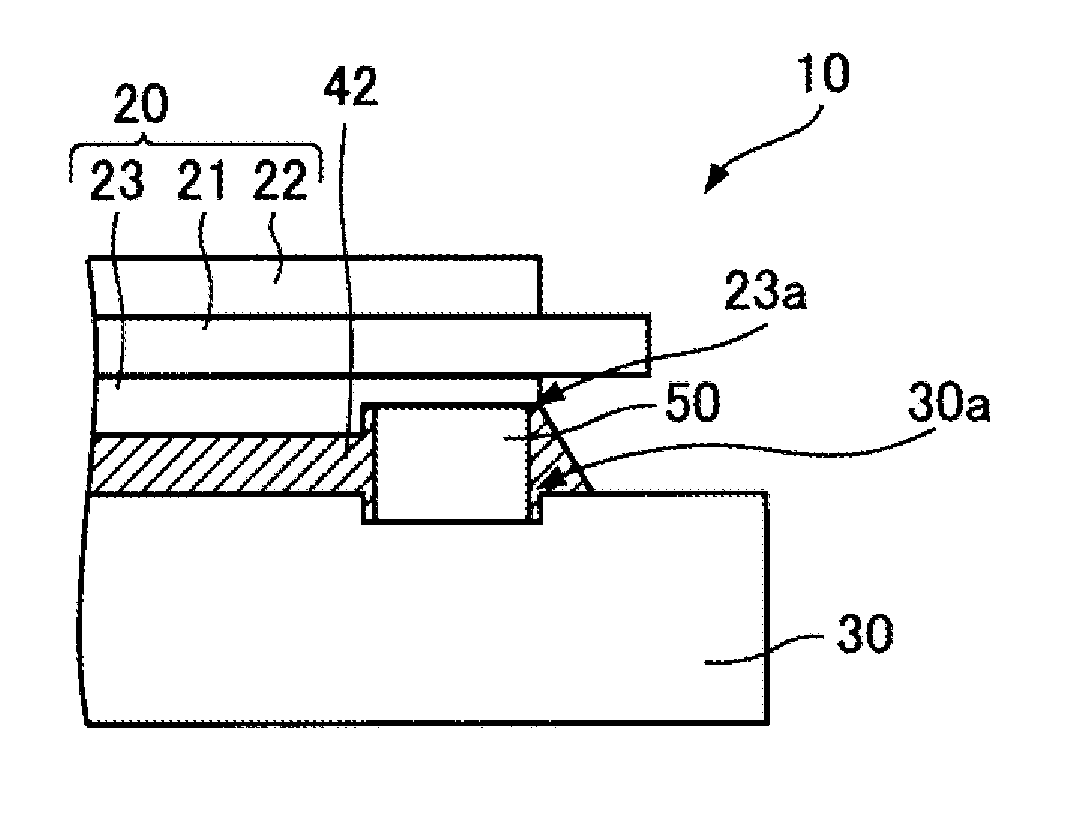
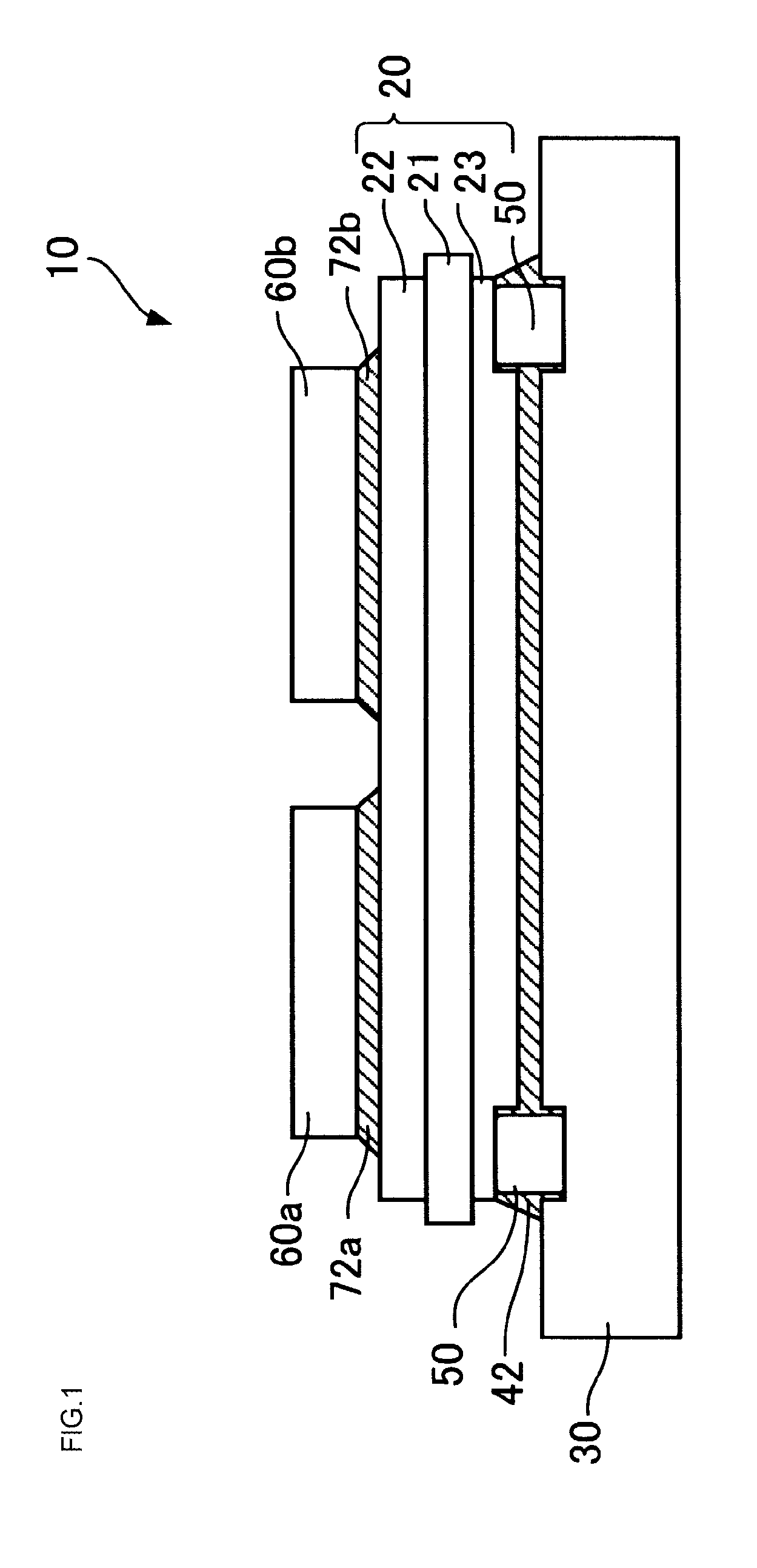
[0024]A description will be given of a semiconductor device of a first embodiment, using FIGS. 1 to 3C.

[0025]FIG. 1 is a sectional view of the semiconductor device of the first embodiment.

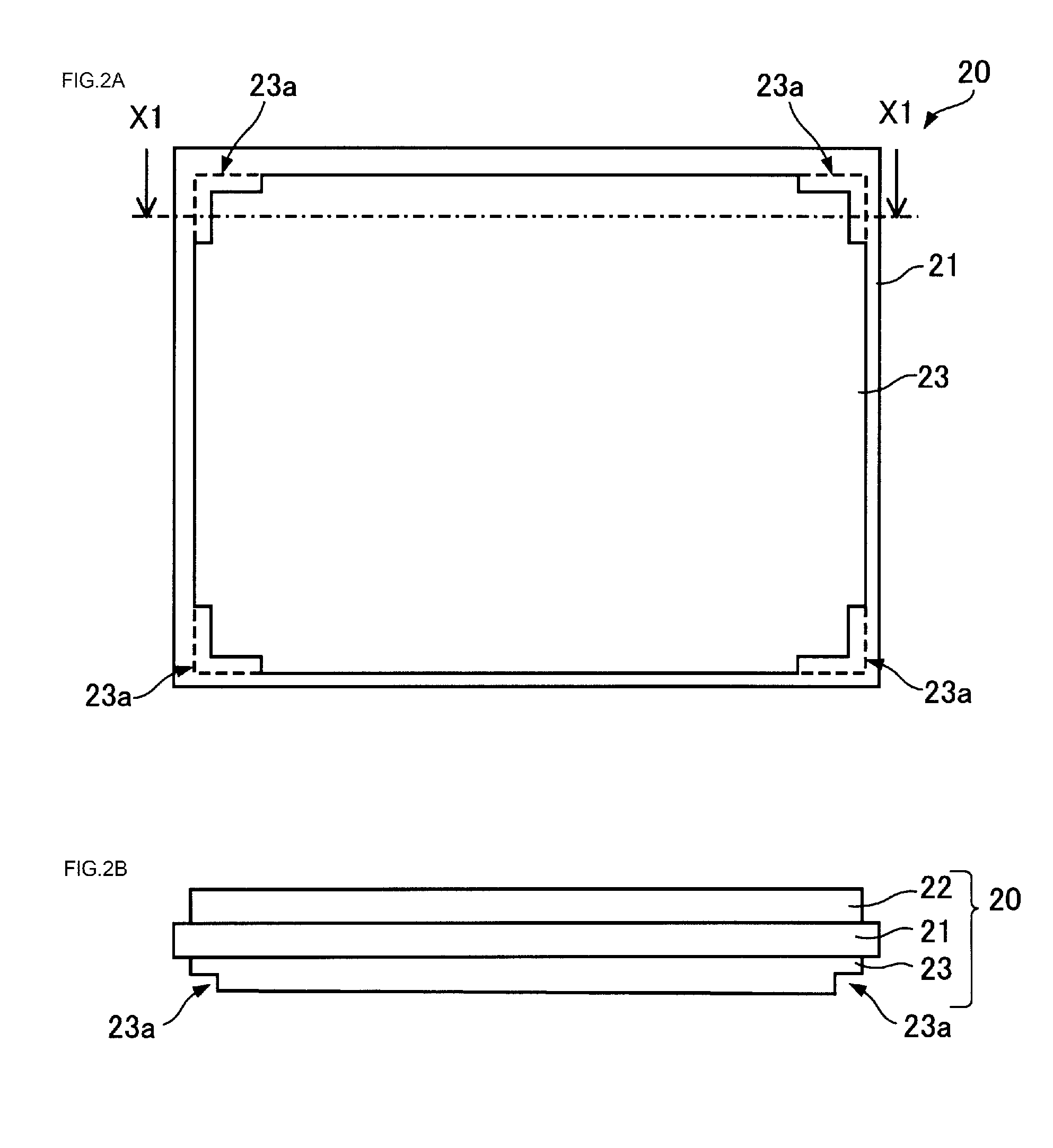
[0026]Also, FIGS. 2A and 2B are diagrams for describing an insulating substrate of the first embodiment. FIG. 2A shows a plan view of the side of the insulating substrate facing a radiating member, while FIG. 2B shows a sectional view taken along a dashed-dotted line X1-X1 of FIG. 2A.

[0027]FIGS. 3A to 3C are diagrams for describing the radiating member of the first embodiment. FIG. 3A shows a plan view of the side of the radiating member facing the insulating substrate, FIG. 3B shows a sectional view taken along a dashed-dotted line X2-X2 of FIG. 3A, and FIG. 3C shows a perspective view of a positioning member. FIGS. 3A and 3B show only one of a plurality of arrangement areas provided on the radiating member.

[0028]A semiconductor device 10 includes semiconductor elements 60a and 60b, an insulating ...

second embodiment

[0075]In a second embodiment, a description will be given of a case wherein a positioning member of another form is applied in the first embodiment. A description of portions duplicating the description of the first embodiment may be omitted.

[0076]FIGS. 9A and 9B are diagrams for describing a semiconductor device of the second embodiment.

[0077]FIG. 9A shows a perspective view of a positioning member of the second embodiment, while FIG. 9B, corresponding to FIG. 8C, shows a sectional view of a corner portion of a semiconductor device using FIG. 9A.

[0078]A positioning member 50a shown in FIG. 9A, in the same way as the positioning member 50, has a surface with high leakage with respect to solder, is of an L-shape in plan view, and includes faces 51a and 52a, and a corner portion Ca configured of the faces 51a and 52a. However, the cross-section of an end portion of the positioning member 50a is a trapezoidal shape wherein sides 50a2 and 50a3 are perpendicular, and a side 50a4 is incli...

third embodiment

[0081]In a third embodiment, a description will be given of a case wherein a positioning member of another shape is still applied in the first embodiment.

[0082]FIGS. 10A and 10B are diagrams for describing a semiconductor device of the third embodiment.

[0083]As the positioning member 50 is formed such that the corner portion C formed from the faces 51 and 52 is positioned in each of the four corners of the insulating substrate 20, the melted solder 41 completely buries the faces 51 and 52 and the corner portion C of the positioning members 50 to reach the four corners of the insulating substrate 20.

[0084]For example, in a semiconductor device 12, a positioning member 50b has a triangular shape in plan view, including faces 51b and 52b, and a corner portion Cb configured of the faces 51b and 52b, as shown in FIG. 10A. In this case, by the faces 51b and 52b, and the corner portion Cb formed from the faces 51b and 52b, being positioned in each of the four corners of the insulating subs...


PUM

PropertyMeasurementUnit
areaaaaaaaaaaa
depthaaaaaaaaaa
L-shapeaaaaaaaaaa

Abstract

A semiconductor device includes a semiconductor element; an insulating substrate formed from stacking a rectangular shaped circuit plate, insulating plate, and metal plate, wherein the semiconductor element is fixed to the circuit plate, and the metal plate has at least one first groove portion in four corners thereof; a radiating member made of metal and having a predetermined arrangement area to dispose the insulating substrate, the radiating member having at least one second groove portion provided in four corners of the arrangement area; four positioning members disposed between the four corners of the metal plate and the four corners of the radiating member, each of the four positioning members being fitted to each of the first groove portions and second groove portions; and a solder filling a space between the insulating substrate and the radiating member, and covering the positioning members.

Description

CROSS-REFERENCE TO RELATED APPLICATION[0001]The present application is a US application claiming priority from Japanese Application No. 2014-144861 filed Jul. 15, 2014, the disclosure of which is incorporated herein.BACKGROUND OF THE INVENTION[0002]1. Field of the Invention[0003]The present invention relates to a semiconductor device and semiconductor device manufacturing method.[0004]2. Description of the Background Art[0005]In a power semiconductor module, a semiconductor chip or the like is fixed with solder to one main surface of an insulating substrate, and a radiating member is fixed with solder to the other main surface of the insulating substrate.[0006]However, in such a power semiconductor module, when the solder repeatedly expands and contracts due to temperature change occurring when operating, notches or the like may occur in the solder. Further, thermal strain concentrates in the notches, whereby fatigue damage occurs in the solder, which may cause breakdown or damage o...

Claims


Application Information

Patent Timeline
Patent Type & Authority Patents(United States)
IPC IPC(8): H01L23/42B23K1/19H01L21/48B23K1/00H01L23/373
CPCB23K1/0016H01L23/3735H01L23/42H01L21/4882B23K1/0006B23K1/19B23K2203/56B23K2203/18B23K2203/12B23K2203/02B23K2203/08H01L2224/32225B23K2103/56B23K2103/02B23K2103/08B23K2103/12B23K2103/18
Inventor SUZUKI, KENJI
Owner FUJI ELECTRIC CO LTD
Learn More