Supercharge Your Innovation With Domain-Expert AI Agents!

Photodetector for imaging system

a photodetector and imaging system technology, applied in the field of semiconductor devices, can solve the problems of physical limitation of the size of the photodetector array that may be manufactured, the need to readout electrical signals, and the limitation of the number of electrical elements at the chip edg

Active Publication Date: 2016-09-06
DETECTION TECH LTD
View PDF24 Cites 3 Cited by
  • Summary
  • Abstract
  • Description
  • Claims
  • Application Information

AI Technical Summary

Benefits of technology

The described invention allows for a larger contact opening in a via than would be possible with just a high aspect ratio opening. This results in a larger contact surface area for contact between a metal contact layer and the conductive material filling the via, which leads to better contact resistance.

Problems solved by technology

In CT detector constructions, a major limiting factor in providing more detector elements is the need to readout the electrical signals from the individual photo-detectors of the detector array.
Using this method, there is a physical limitation on the size of a photo-detector array that may be manufactured.
The number of electrical elements at the chip edge is limited, and this limits the number of photo-detector elements which can be connected.
Because of the need to accommodate the physical wires and their connections, the number of photo-detectors in an array is limited.
In particular, it is not possible to add further photo-detectors in the z direction.

Method used


Image

  • Photodetector for imaging system
  • Photodetector for imaging system
  • Photodetector for imaging system

Examples


Embodiment Construction

[0074]The present invention is described hereinafter with reference to a particular set of embodiments. However the invention is not limited to such embodiments.

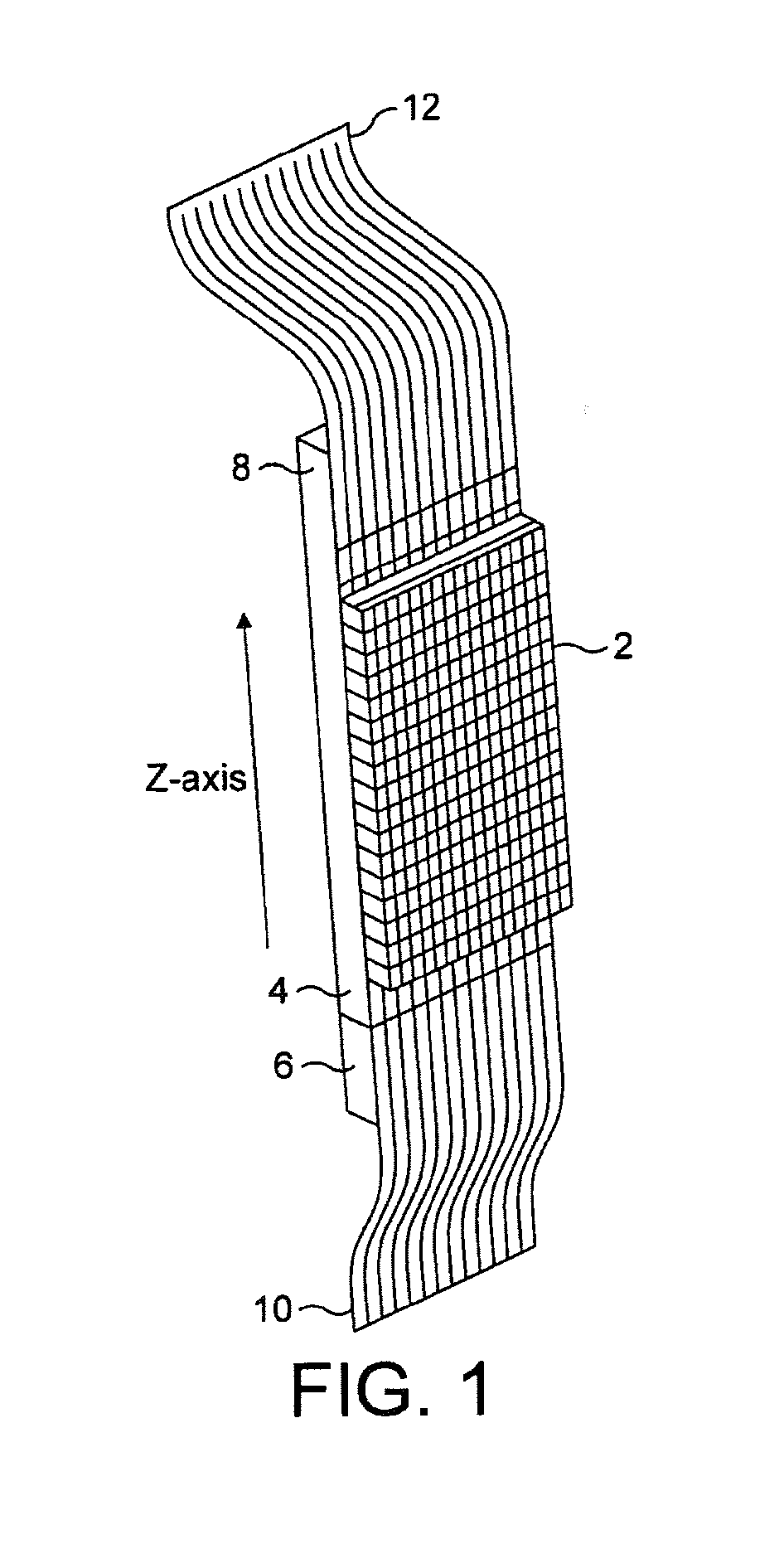
[0075]The invention is particularly described herein with reference to an example of a photodetector array for a CT medical imaging system. The invention, and embodiments thereof, are however not limited to such applications.

[0076]Whilst the invention is illustrated herein by way of reference to various figures, none of these figures are drawn to scale, but rather are drawn to best illustrate various features of the present invention.

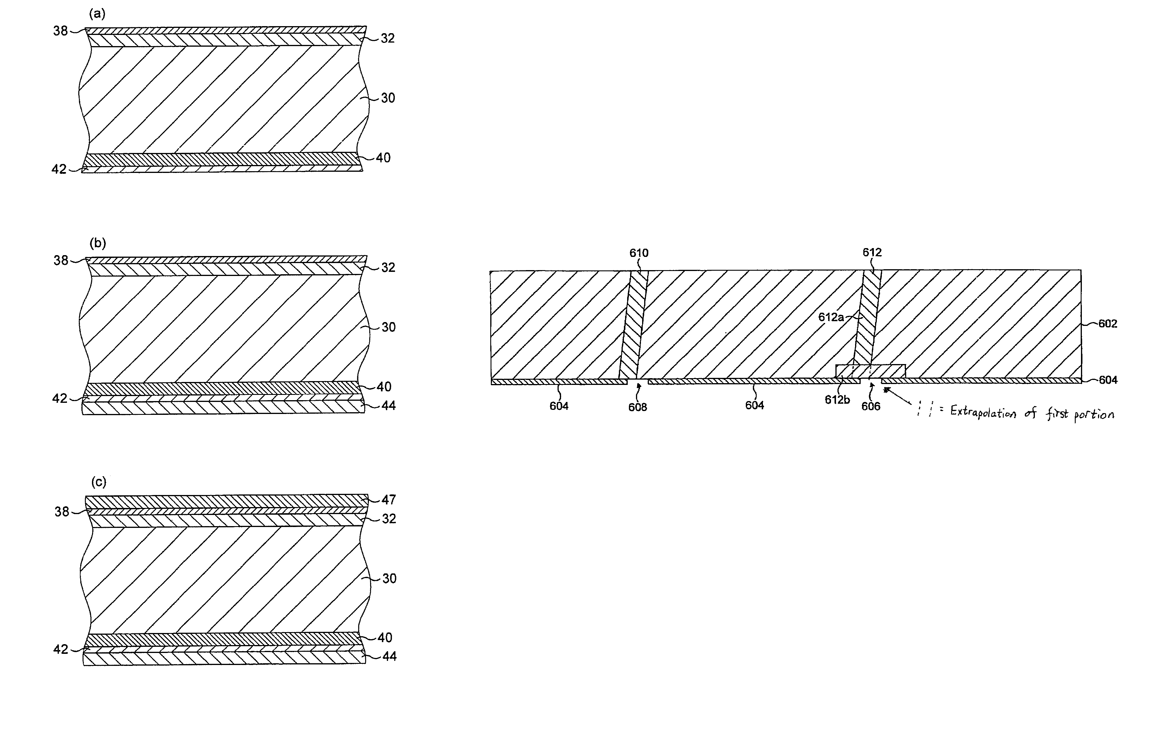
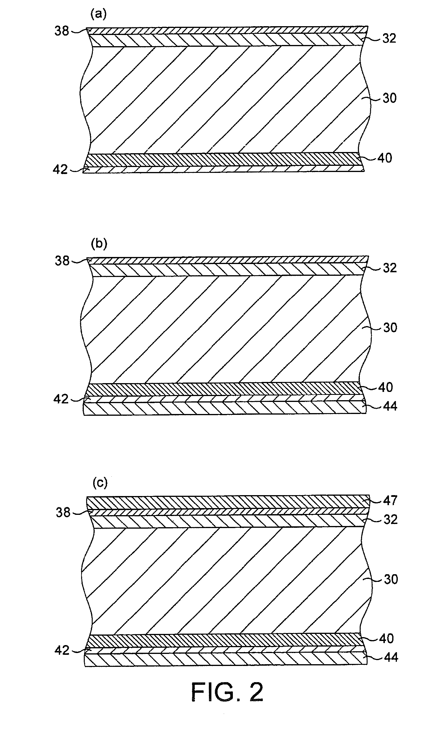
[0077]With reference to FIGS. 2(a) to 2(n), there are illustrated selected steps for manufacturing a photo-detector array for a CT imaging system in accordance with a preferred embodiment of the invention. A cross-section through an exemplary device substrate is used for the purpose of explaining the present invention. Only those steps relevant to an understanding of the present invention are sh...


PUM


Abstract

There is disclosed a substrate including at least one photodetector, the photodetector having a first active area on a first surface of the substrate and a second active area on a second surface of the substrate, wherein the photodetector is provided with a conductive via electrically isolated from the substrate, said conductive via extending through the photodetector from the first surface of the substrate to the second surface of the substrate for connecting the first active area to the second surface of the substrate, the second surface providing electrical connections for the first and second active areas of the photodetector.

Description

[0001]The present application claims priority to the international patent application identified as PCT / EP2008 / 056933 filed on Jun. 4, 2008, which itself claims priority to the UK patent application identified as GB 0710629.7 filed on Jun. 4, 2007, the disclosures of which are both incorporated herein by reference in their entirety.FIELD OF THE INVENTION[0002]The present invention relates to semiconductor devices having active areas formed on both sides of a substrate, and particularly but not exclusively to photo-detectors for use in imaging systems.BACKGROUND OF THE INVENTION[0003]Photo-detectors are used in imaging systems for medical, security and industrial applications. One particular medical application of photo-detectors is in computed tomography (CT) systems.[0004]In a typical CT system, an X-ray source with a fan-shaped X-ray beam and a two-dimensional radiation detector array are assembled on a mechanical support structure, known as a gantry. In use, the gantry is rotated...

Claims


Application Information

Patent Timeline
Patent Type & Authority Patents(United States)
IPC IPC(8): H01L27/146H01L21/768
CPCH01L27/14634H01L21/76898H01L27/14658H01L2924/0002H01L2924/00G01T1/24H01L23/481H01L27/14636A61B6/035A61B6/4233
Inventor JI, FANJUNTUNEN, MIKKOHIETANEN, IIRO
Owner DETECTION TECH LTD
Features
  • R&D
  • Intellectual Property
  • Life Sciences
  • Materials
  • Tech Scout
  • Unparalleled Data Quality
  • Higher Quality Content
  • 60% Fewer Hallucinations
Learn More