Etching method for reducing microloading effect
- Summary
- Abstract
- Description
- Claims
- Application Information
AI Technical Summary
Benefits of technology
Problems solved by technology
Method used
Image

Examples
Embodiment Construction
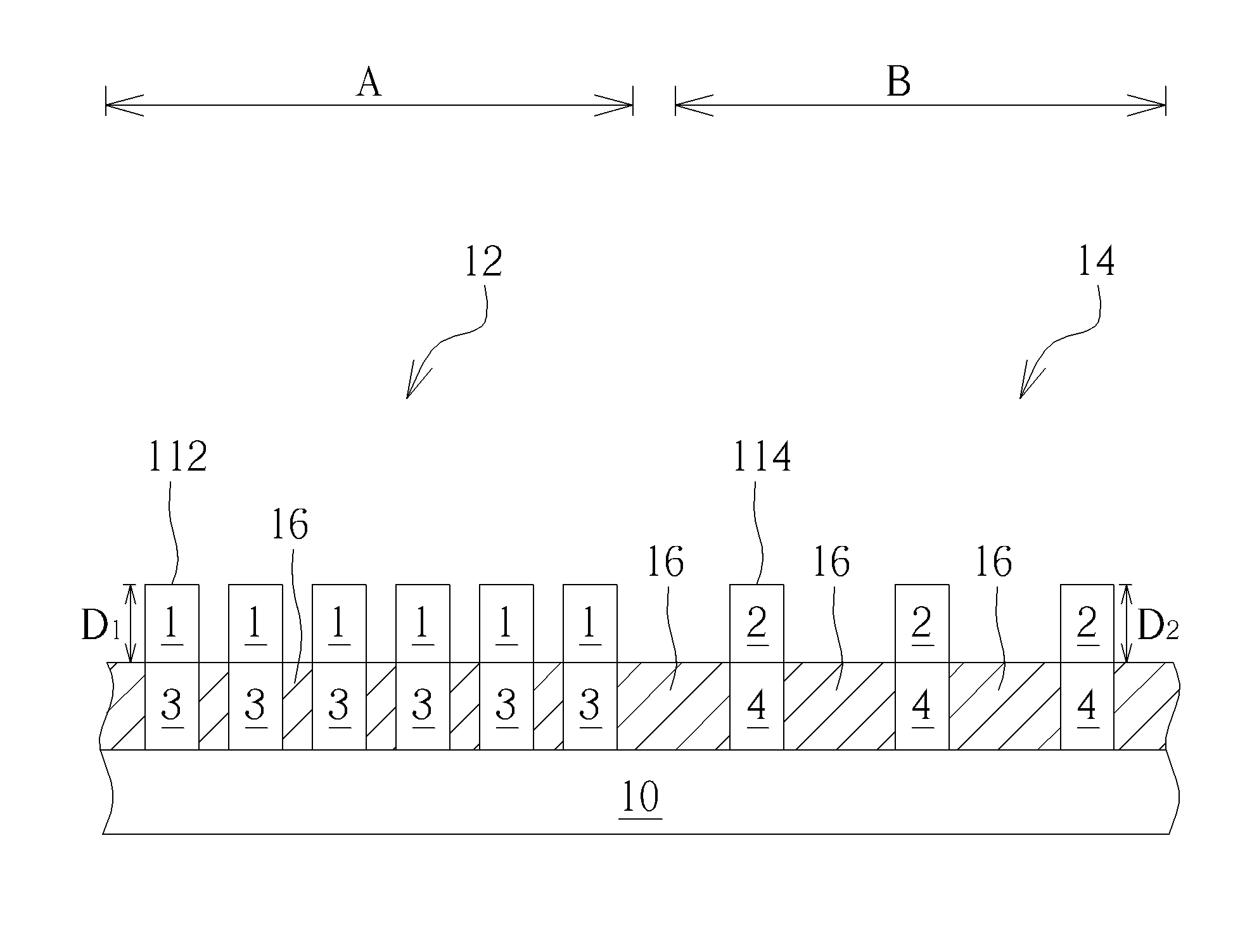
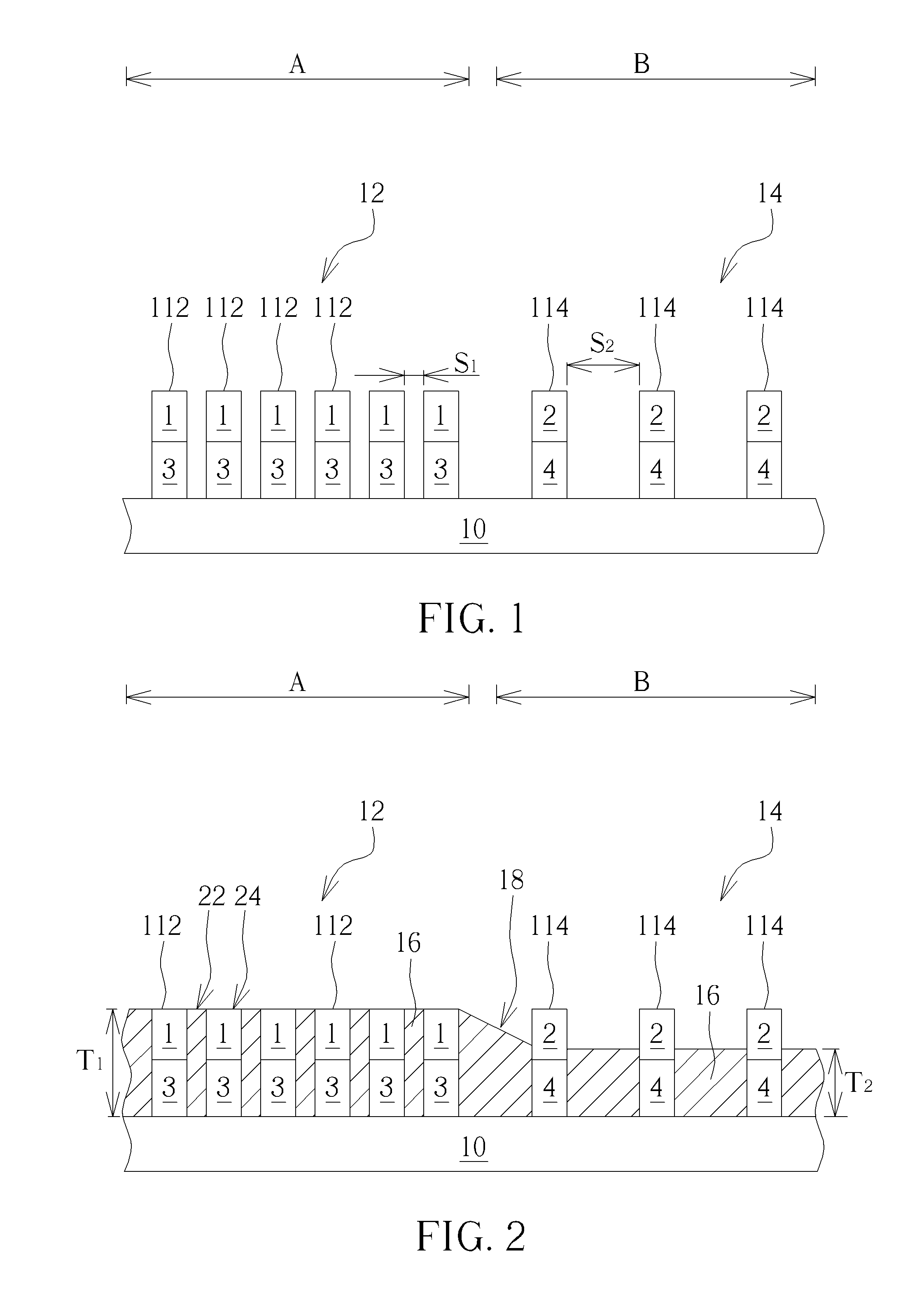
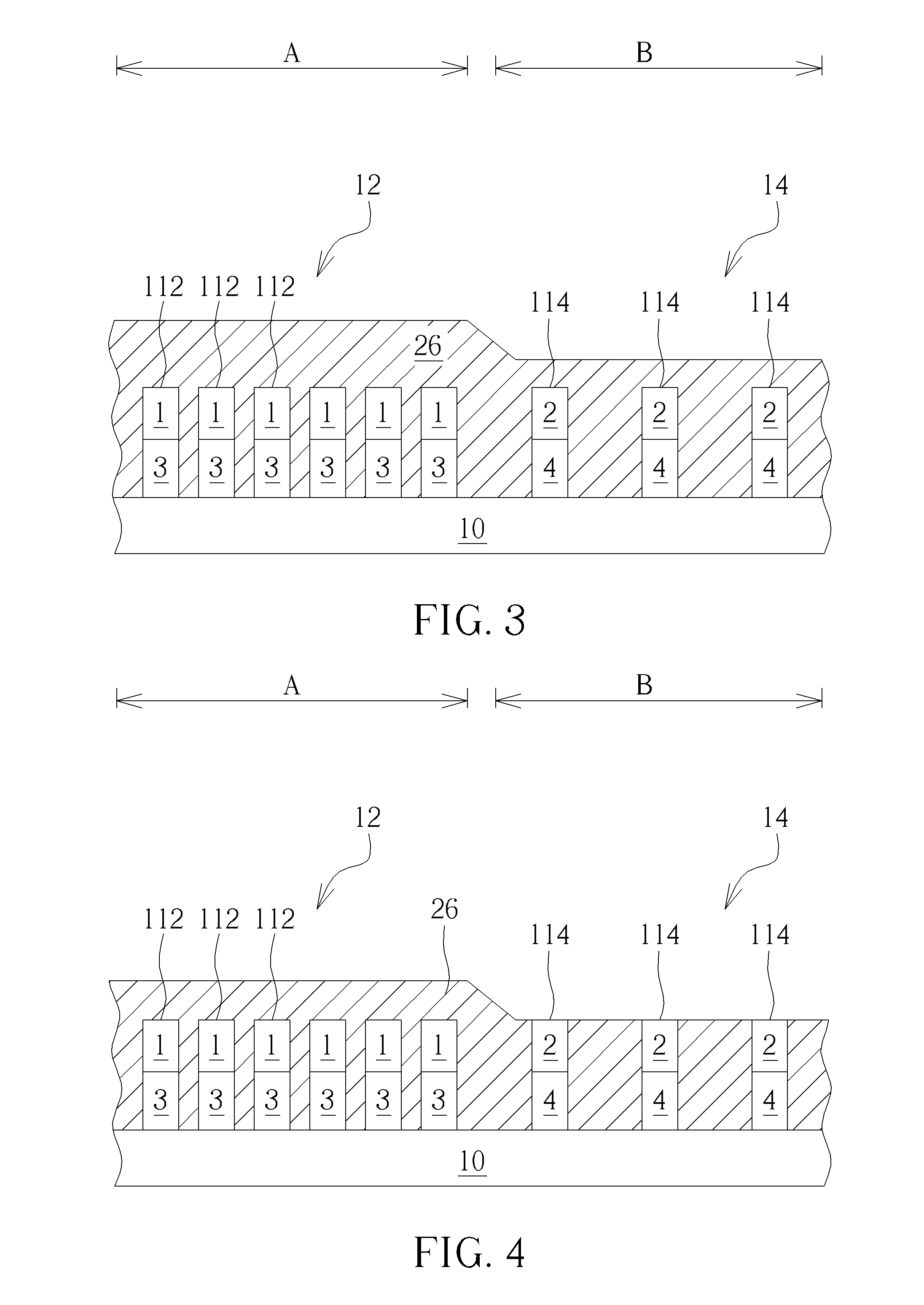
[0012]FIGS. 1 to 8 depict an etching method according to a preferred embodiment of the present invention. The etching step and the etching back step used in the present invention can be dry etching, wet etching or a combination of both. As shown in FIG. 1, a substrate 10 is provided. The substrate 10 can be a bulk silicon substrate, a germanium substrate, a gallium arsenide substrate, a silicon germanium substrate, an indium phosphide substrate, a gallium nitride substrate, a silicon carbide substrate, or a silicon on insulator (SOI) substrate. The substrate 10 is defined into a high density region A and a low density region B. A high density structure 12 is disposed on the substrate 10 and within the high density region A. The high density structure 12 includes numerous first structures 112. A first space S1 is between adjacent first structures 112. A low density structure 14 is disposed on the substrate 10 and within the low density region B. The low density structure 14 includes ...
PUM
 Abstract
Description
Claims
Application Information