
Photoelectric wiring module

a photoelectric wiring and photoelectric technology, applied in the field of photoelectric wiring modules, can solve the problems of copper-based wirings, wiring miniaturization, and inability to meet the needs of high-speed transmission of large amounts of data, and achieve the effects of ensuring the reliability of optical coupling, ensuring mass productivity, and ensuring physical stability of mounting components

Active Publication Date: 2016-09-20
LS MTRON LTD
View PDF18 Cites 0 Cited by
  • Summary
  • Abstract
  • Description
  • Claims
  • Application Information

AI Technical Summary

Benefits of technology

[0029]According to the present invention as described above, devices and components of a photoelectric wiring module can be used without any modification such as an additional processing process, the photoelectric wiring module can be easily produced in large quantities, and a process of mounting the devices and components on a substrate is facilitated to ensure mass productivity, such as manufacturing speed, etc. Furthermore, a process of processing a mirror surface of an optical transmission line need not be performed.
[0030]In addition, the present invention provides a horizontal alignment structure between an optical device package and the optical transmission line. Thus, the optical device package and the optical transmission line can be butt-coupled at a close distance with each other without an additional member, such as a lens, a mirror, or the like. During the coupling of the optical device package with the optical transmission line, passive alignment may be performed instead of an active alignment process of adjusting a position while taking measurements using a measuring apparatus. Also, optical coupling reliability and physical stability for mounting components can be ensured.
[0031]Also, since the photoelectric wiring module according to the present invention has the horizontal alignment structure instead of a vertical alignment structure, an optical coupling distance can be minimized to promote reliability of optical alignment.
[0032]In addition, the photoelectric wiring module according to the present invention is structured such that a frame functioning as an electrical connector is mounted on the substrate and an electrical component and an optical component are disposed within the frame. Thus, miniaturization and low height can be promoted.
[0033]Also, the present invention can be easily applied to an inner board of an applied product and ensure performance and reliability, thereby enabling commercialization of the photoelectric wiring module.
[0034]In addition, since the present invention provides a double contact structure during the mating of the plug with the receptacle, electrical connection reliability of the photoelectric wiring module can be ensured.

Problems solved by technology

Thus, signal attenuation, noise, electromagnetic interference (EMI) / electromagnetic compatibility (EMC), impedance matching, crosstalk, skew, connection wiring miniaturization, etc. have been highlighted as big issues.
However, the copper-based wirings neither meet the needs of high-speed transmission of large amounts of data nor solve various technical issues in accordance with the above-described latest trends in electronic apparatuses.

Method used


Image

  • Photoelectric wiring module
  • Photoelectric wiring module
  • Photoelectric wiring module

Examples


Embodiment Construction

[0044]The objects, features, and advantages of the present invention will be apparent from the following detailed description of embodiments of the invention with references to the following drawings, so that the disclosure can be easily implemented by one skilled in the art. Descriptions of well-known components and processing techniques are omitted so as not to unnecessarily obscure the embodiments of the present invention. The present invention will now be described more fully with reference to the accompanying drawings, in which exemplary embodiments of the invention are shown.

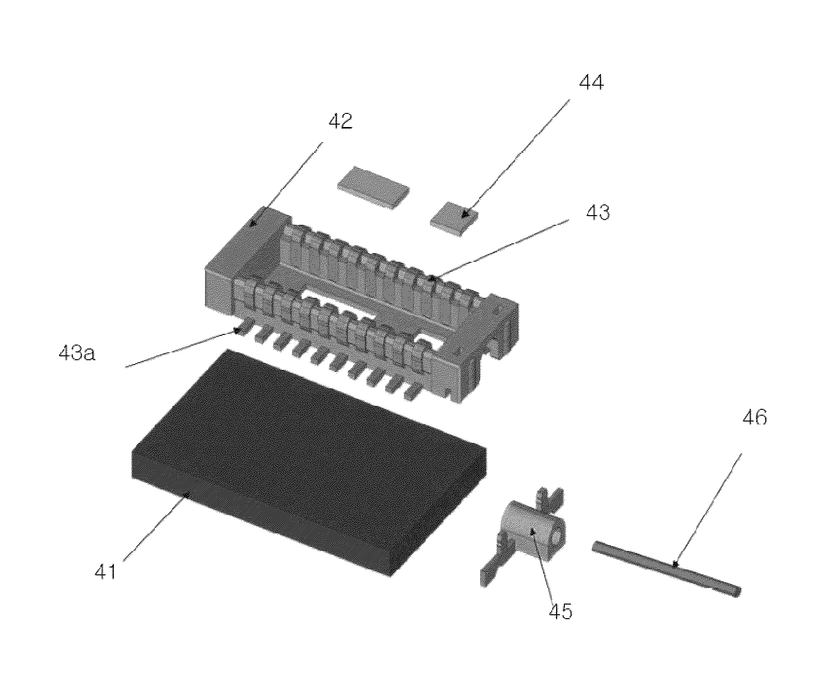
[0045]FIG. 4 is a perspective view of a photoelectric wiring module according to an exemplary embodiment of the present invention, FIG. 5 is an exploded view of the photoelectric wiring module of FIG. 4, FIG. 6 is perspective views of an optical device package proposed in the present invention, and FIG. 7 is assembly diagrams of a process of manufacturing a photoelectric wiring module according to the pres...


PUM


Abstract

Disclosed is a photoelectric wiring module which includes: a substrate; a frame mounted on the substrate; an optical device package configured to perform photoelectric conversion or electro-optic conversion of a signal; an optical control device configured to control an operation of the optical device package; and an optical transmission line configured to transmit an optical signal that is emitted from the optical device package or incident on the optical device package. Electrical terminals are disposed on the frame, the optical device package is mounted on the frame, and the optical control device is disposed within the frame and mounted on the substrate.

Description

CROSS REFERENCE TO PRIOR APPLICATIONS[0001]This application is a National Stage Application of PCT International Patent Application No. PCT / KR2012 / 010226 filed on Nov. 29, 2012, under 35 U.S.C. §371, which claims priority to Korean Patent Application No. 10-2011-0126145 filed on Nov. 29, 2011, which are all hereby incorporated by reference in their entirety.TECHNICAL FIELD[0002]The present invention relates to a photoelectric wiring module, and more particularly, to a photoelectric wiring module for transmitting a massive amount of data between boards in apparatuses at a high speed. In particular, the present invention relates to a photoelectric wiring module that is based on an optical device package (e.g., a vertical-cavity surface-emitting laser package (VCSEL PKG) and a photodiode PKG (PD PKG)) having a vertical alignment structure for butt-coupling and passive-alignment.BACKGROUND ART[0003]Thanks to the development of IT technology, high performance, acceleration, high integrat...

Claims


Application Information

Patent Timeline
Patent Type & Authority Patents(United States)
IPC IPC(8): G02B6/36G02B6/12G02B6/43G02B6/42
CPCG02B6/12G02B6/426G02B6/4242G02B6/4245G02B6/4257G02B6/4286G02B6/43G02B6/42
Inventor LEE, SEUNG-HUNSONG, IN-DUCKPARK, KEON-CHEOLLEE, ICK-KYUN
Owner LS MTRON LTD
Learn More