

Method for fabricating semiconductor devices
a semiconductor device and manufacturing method technology, applied in the direction of semiconductor devices, electrical devices, chemistry apparatus and processes, etc., can solve the problem of difficult to implement the greater integration of semiconductor devices
- Summary
- Abstract
- Description
- Claims
- Application Information
AI Technical Summary
Benefits of technology
Problems solved by technology
Method used
Image

Examples
Embodiment Construction
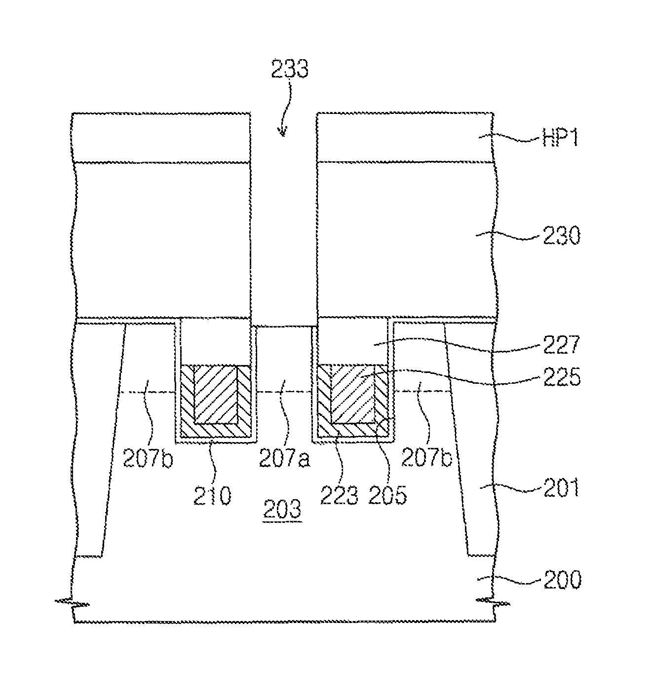
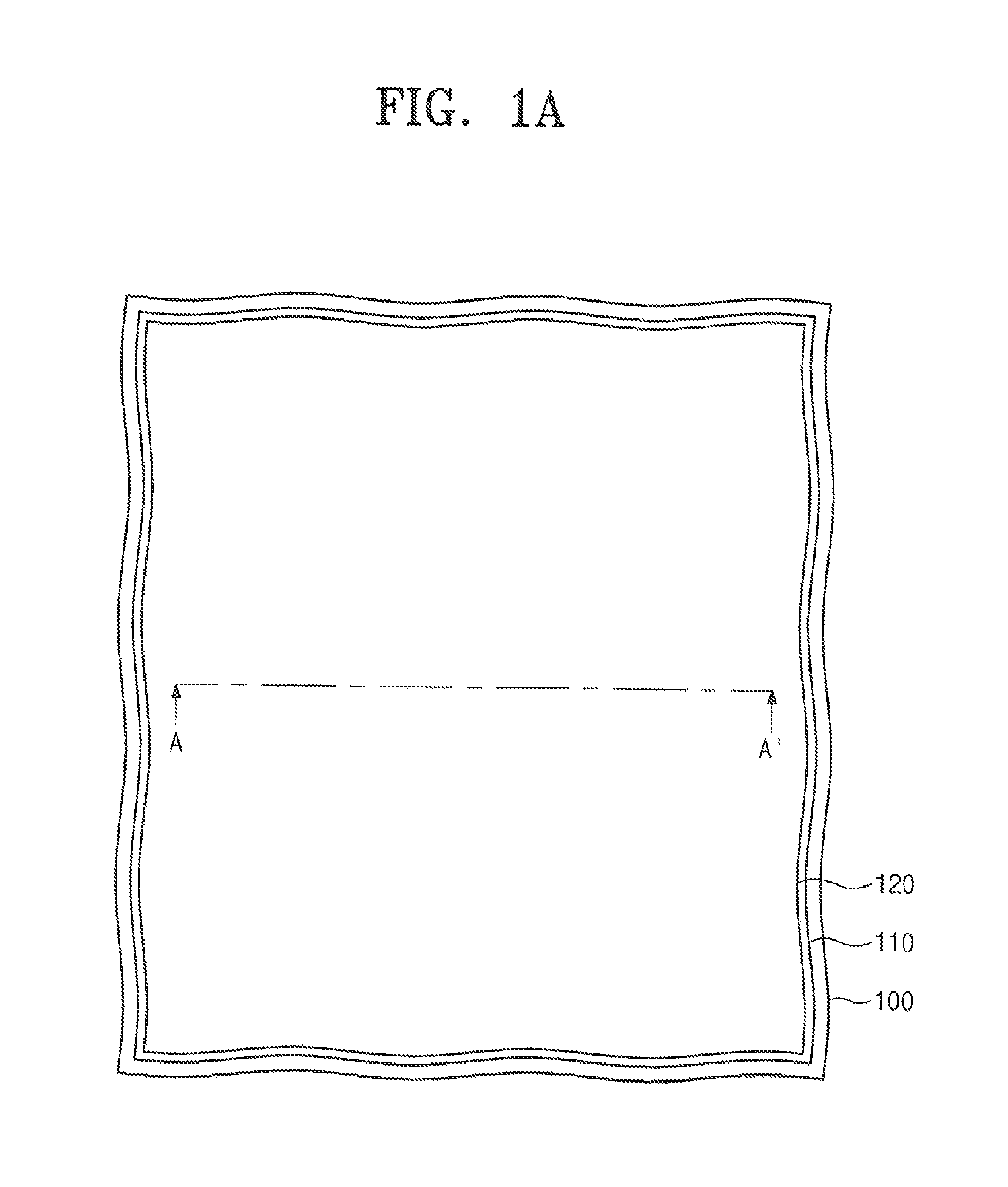
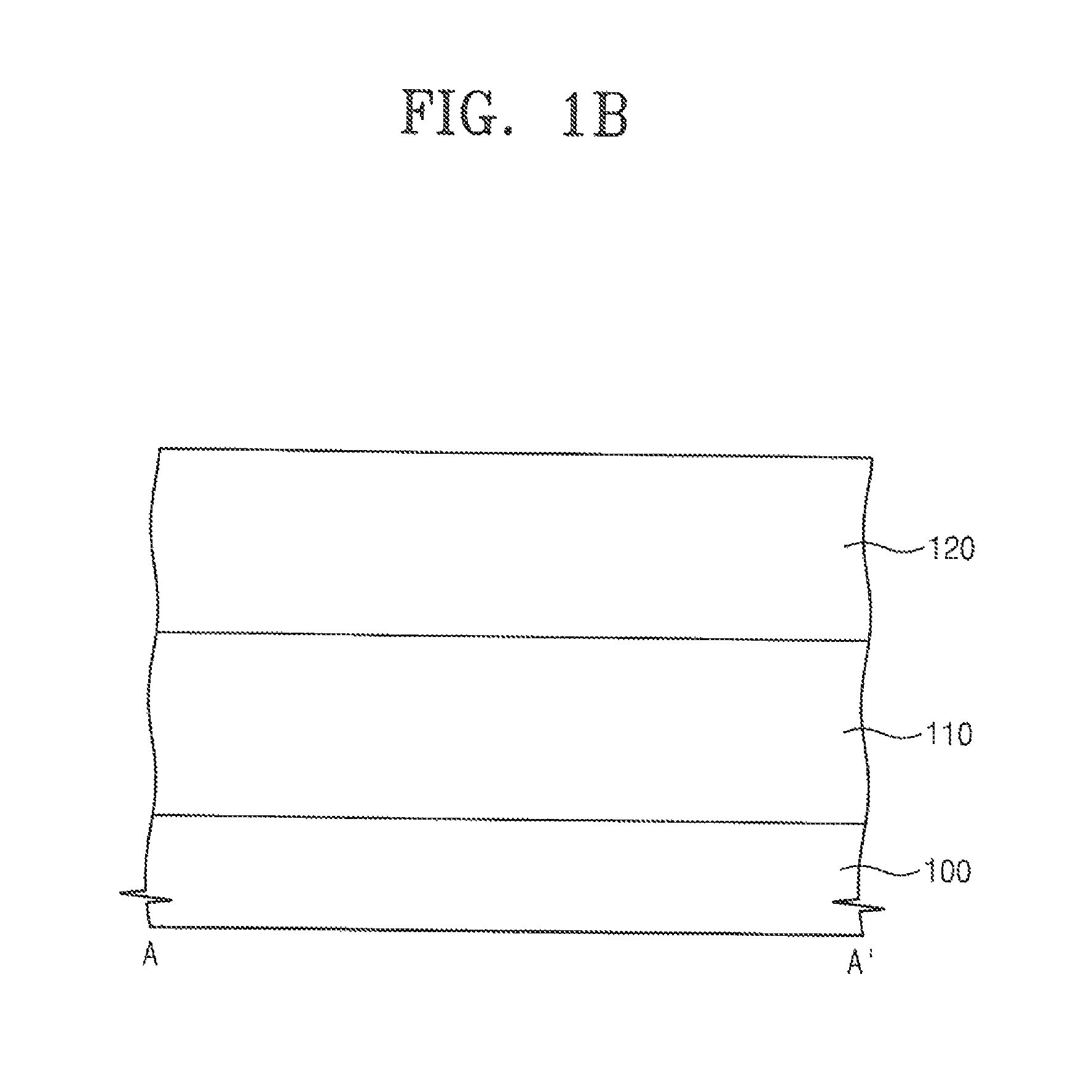
[0041]Embodiments of inventive concepts will now be described more fully hereinafter with reference to the accompanying drawings, in which some exemplary embodiments of inventive concepts are shown. These embodiments, however, should not be construed as being limited to the exemplary embodiments more particularly set forth herein; rather, these embodiments are provided so that this disclosure will be thorough and complete, and will fully convey the scope of these embodiments of inventive concepts to those of skill in the art. In the drawings, the thicknesses of layers and regions are exaggerated for clarity. Like reference numerals in the drawings denote like elements. Hereinafter, exemplary embodiments of the present invention will be described in conjunction with the accompanying drawings.
[0042]The terminology used herein is for the purpose of describing particular embodiments only and is not intended to be limiting of the invention. As used herein, the singular forms “a,”“an” and...
PUM
| Property | Measurement | Unit |
|---|---|---|
| temperature | aaaaa | aaaaa |
| pressure | aaaaa | aaaaa |
| aspect ratio | aaaaa | aaaaa |
Abstract
Description
Claims
Application Information